HCF4021B
ASYNCHRONOUS PARALLEL IN OR SYNCHRONOUS
SERIAL IN/SERIAL OUT 8 - STAGE STATIC SHIFT REGISTER
s
s
s
s
s
s
s
s
MEDIUM SPEED OPERATION : 12 MHz
(Typ.) CLOCK RATE AT V
DD
- V
SS
= 10V
FULLY STATIC OPERATION
8 MASTER-SLAVE FLIP-FLOPS PLUS
OUTPUT BUFFERING AND CONTROL
GATING
QUIESCENT CURRENT SPECIFIED UP TO
20V
5V, 10V AND 15V PARAMETRIC RATINGS
INPUT LEAKAGE CURRENT
I
I
= 100nA (MAX) AT V
DD
= 18V T
A
= 25擄C
100% TESTED FOR QUIESCENT CURRENT
MEETS ALL REQUIREMENTS OF JEDEC
JESD13B " STANDARD SPECIFICATIONS
FOR DESCRIPTION OF B SERIES CMOS
DEVICES"
DIP
SOP
ORDER CODES
PACKAGE
DIP
SOP
TUBE
HCF4021BEY
HCF4021BM1
T&R
HCF4021M013TR
DESCRIPTION
The HCF4021B is a monolithic integrated circuit
fabricated in Metal Oxide Semiconductor
technology available in DIP and SOP packages.
This device is an 8-stage parallel or serial input/
serial output register having common CLOCK and
PARALLEL/SERIAL CONTROL inputs, a single
SERIAL data input, and individual parallel "JAM"
inputs to each register stage. Each register stage
is a D-type, master-slave flip-flop in addition to an
output from stage 8, "Q" outputs are also available
from stages 6 and 7. Serial entry is synchronous
with the clock but parallel entry is asynchronous.
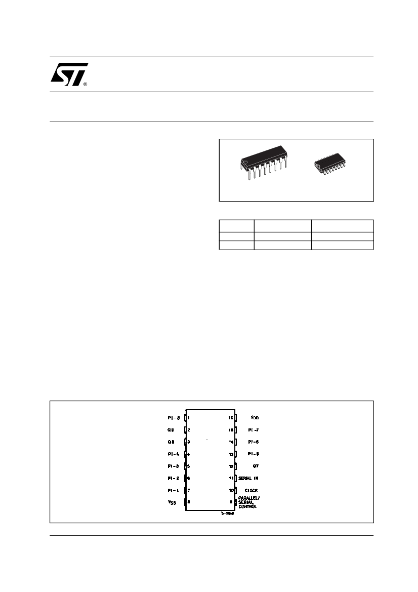
PIN CONNECTION
In this device, entry is controlled by the
PARALLEL/SERIAL CONTROL input. When the
PARALLEL/SERIAL CONTROL input is low, data
is serially shifted into the 8-stage register
synchronously with the positive transition of he
clock line. When the PARALLEL/SERIAL
CONTROL input is high, data is jammed into the
8-stage register via the parallel input lines and
synchronous with the positive transition of the
clock line, the CLOCK input of the internal stage is
"forced" when asynchronous parallel entry is
made. Register expansion using multiple package
is permitted.
September 2001
1/11


 1
1
 2
2
 3
3
 4
4
 5
5
 6
6
 7
7
 8
8
 9
9
 10
10
 11
11
