HAF70009
Data Sheet
August 1999
File Number
4770
56A, 100V, 0.025 Ohm, N-Channel
UltraFET Power MOSFET
This N-Channel power MOSFET is
manufactured using the innovative
UltraFET鈩?process. This advanced
process technology achieves the
lowest possible on-resistance per silicon area, resulting in
outstanding performance. This device is capable of
withstanding high energy in the avalanche mode and the
diode exhibits very low reverse recovery time and stored
charge. It was designed for use in applications where power
ef鏗乧iency is important, such as switching regulators,
switching converters, motor drivers, relay drivers, low-
voltage bus switches, and power management in portable
and battery-operated products.
Formerly developmental type TA75639.
Features
鈥?56A, 100V
鈥?Simulation Models
- Temperature Compensated PSPICE
廬
and SABER
漏
Electrical Models
- Spice and Saber Thermal Impedance Models
- www.intersil.com
鈥?Peak Current vs Pulse Width Curve
鈥?UIS Rating Curve
鈥?Related Literature
- TB334, 鈥淕uidelines for Soldering Surface Mount
Components to PC Boards鈥?/div>
Symbol
D
Ordering Information
PART NUMBER
HAF70009
PACKAGE
TO-220AB
TEMP. RANGE (
o
C)
-55 to 175
G
S
Packaging
JEDEC TO-220AB
SOURCE
DRAIN
GATE
DRAIN
(FLANGE)
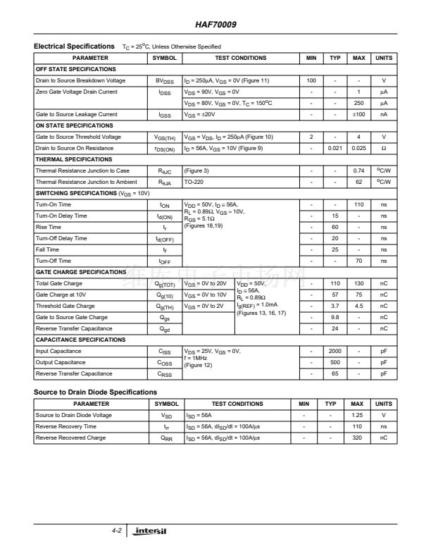
Absolute Maximum Ratings
T
C
= 25
o
C, Unless Otherwise Speci鏗乪d
HAF70009
100
100
鹵20
56
Figure 4
Figures 6, 14, 15
200
1.35
-55 to 175
300
260
UNITS
V
V
V
A
Drain to Source Voltage (Note 1) . . . . . . . . . . . . . . . . . . . . . . . . . . . . . . . . . . . . . . . . . . . . . . . V
DSS
Drain to Gate Voltage (R
GS
= 20k鈩? (Note 1) . . . . . . . . . . . . . . . . . . . . . . . . . . . . . . . . . . . . . V
DGR
Gate to Source Voltage . . . . . . . . . . . . . . . . . . . . . . . . . . . . . . . . . . . . . . . . . . . . . . . . . . . . . . . V
GS
Drain Current
Continuous (Figure 2). . . . . . . . . . . . . . . . . . . . . . . . . . . . . . . . . . . . . . . . . . . . . . . . . . . . . . . . . I
D
Pulsed Drain Current . . . . . . . . . . . . . . . . . . . . . . . . . . . . . . . . . . . . . . . . . . . . . . . . . . . . . . . I
DM
Pulsed Avalanche Rating . . . . . . . . . . . . . . . . . . . . . . . . . . . . . . . . . . . . . . . . . . . . . . . . . . . . . . E
AS
Power Dissipation . . . . . . . . . . . . . . . . . . . . . . . . . . . . . . . . . . . . . . . . . . . . . . . . . . . . . . . . . . . . P
D
Derate Above 25
o
C . . . . . . . . . . . . . . . . . . . . . . . . . . . . . . . . . . . . . . . . . . . . . . . . . . . . . . . . . . .
Operating and Storage Temperature . . . . . . . . . . . . . . . . . . . . . . . . . . . . . . . . . . . . . . . . . T
J
, T
STG
Maximum Temperature for Soldering
Leads at 0.063in (1.6mm) from Case for 10s. . . . . . . . . . . . . . . . . . . . . . . . . . . . . . . . . . . . . . T
L
Package Body for 10s, See Tech Brief 334 . . . . . . . . . . . . . . . . . . . . . . . . . . . . . . . . . . . . . . T
pkg
W
W/
o
C
o
C
o
C
o
C
CAUTION: Stresses above those listed in 鈥淎bsolute Maximum Ratings鈥?may cause permanent damage to the device. This is a stress only rating and operation of the
device at these or any other conditions above those indicated in the operational sections of this speci鏗乧ation is not implied.
NOTE:
1. T
J
= 25
o
C to 150
o
C.
4-1
CAUTION: These devices are sensitive to electrostatic discharge; follow proper IC Handling Procedures.
http://www.intersil.com or 407-727-9207 | Copyright 漏 Intersil Corporation 1999. SABER漏 is a Copyright of Analogy, Inc.
UltraFET鈩?is a trademark of Intersil Corporation. PSPICE廬 is a registered trademark of MicroSim Corporation.


 1
1
 2
2
 3
3
 4
4
 5
5
 6
6
 7
7
 8
8
 9
9
 10
10
