HI-SINCERITY
MICROELECTRONICS CORP.
Spec. No. : MOS200501
Issued Date : 2005.01.01
Revised Date : 2005.09.28
Page No. : 1/5
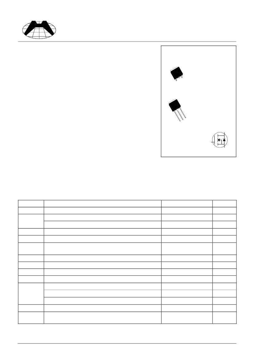
H01N60S Series
N-Channel Power Field Effect Transistor
H01N60S Series Pin Assignment
Tab
Description
This high voltage MOSFET uses an advanced termination scheme to
provide enhanced voltage-blocking capability without degratding
performance over time. In addition, this advanced MOSFET is designed to
withstand high energy in avalanche and commutation modes. The new
energy efficient design also offers a drain-to-source diode with a fast
recovery time. Designed for high voltage, high speed switching
applications in power supplies, converters and PWM motor controls,
these devices are particularly well suited for bridge circuits where diode
speed and commutating safe operating areas are critical and offer
additional and saafety margin against unexpected voltage transients.
Tab
1
2
3
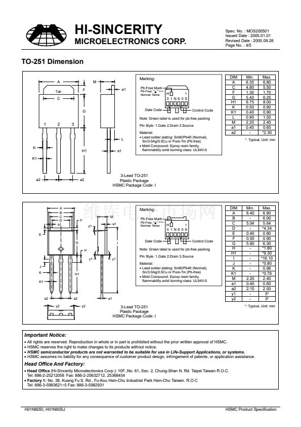
3-Lead Plastic
TO-252
Package Code: J
Pin 1: Gate
Pin 2 & Tab: Drain
Pin 3: Source
1
2
3
3-Lead Plastic
TO-251
Package Code: I
Pin 1: Gate
Pin 2 & Tab: Drain
Pin 3: Source
D
Features
鈥?/div>
1A, 600V, R
DS(on)
=12鈩V
GS
=10V
鈥?/div>
Low Gate Charge 15nC(Typ.)
鈥?/div>
Low C
rss
4pF(Typ.)
鈥?/div>
Fast Switching
鈥?/div>
Improved d
v
/d
t
Capability
H01N60S Series
Symbol:
G
S
Absolute Maximum Ratings
Symbol
V
DSS
I
D
I
DM
V
GS
E
AS
I
AR
E
AR
dv/dt
V
GS
P
D
T
j
, T
stg
T
L
Drain-Source Voltage
Drain Current (Continuous T
C
=25
o
C)
Drain Current (Continuous T
C
=100
o
C)
Drain Current (Pulsed)
*1
Gate-Source Voltage
Single Pulse Avalanche Energy
(L=59mH, I
AS
=1.1A, V
DD
=50V, R
G
=25鈩? Starting T
J
=25擄C)
Avalanche Current
*1
Repetitive Avalanche Energy
Peak Diode Recovery dv/dt
*2
Gate-to-Source Voltage (Continue)
Total Power Dissipation (T
A
=25
o
C)
Total Power Dissipation (T
C
=25
o
C)
Derate above 25擄C
Operating and Storage Temperature Range
Maximum Lead Temperature for Soldering Purposes, 1/8鈥?/div>
from case for 5 seconds
Parameter
H01N60SI / H01N60SJ
600
1
0.6
4
鹵30
50
1
2.8
4.5
鹵20
2.5
28
0.22
-55 to +150
300
Units
V
A
A
A
V
mJ
A
mJ
V/nS
V
W
W
W/擄C
擄C
擄C
*1: Repetitive Rating : Pulse width limited by maximum junction temperature
*2: I
SD
鈮?.1A,
di/dt鈮?00A/us, V
DD
鈮V
DSS
, Starting TJ=25
o
C
H01N60SI, H01N60SJ
HSMC Product Specification
H01N60S相關(guān)型號PDF文件下載
-
型號
版本
描述
廠商
下載
-
英文版
N-Channel Power Field Effect Transistor
HSMC [Hi-S...
-
英文版
N-Channel Power Field Effect Transistor
HSMC
-
英文版
N-Channel Power Field Effect Transistor
HSMC [Hi-S...
-
英文版
N-Channel Power Field Effect Transistor
HSMC [Hi-S...
-
英文版
N-Channel Power Field Effect Transistor
HSMC [Hi-S...
-
英文版
N-Channel Power Field Effect Transistor
HSMC
-
英文版
N-Channel Power Field Effect Transistor
HSMC [Hi-S...
-
英文版
N-Channel Power Field Effect Transistor
HSMC
-
英文版
N-Channel Power Field Effect Transistor
HSMC [Hi-S...
-
英文版
N-Channel Power Field Effect Transistor
HSMC
-
英文版
N-Channel Power Field Effect Transistor
HSMC [Hi-S...


 1
1
 2
2
 3
3
 4
4
 5
5
