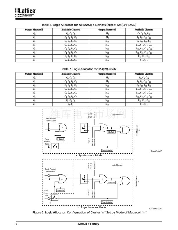
G R O A TH R U G R O M
S U R FA C E M O U N T G L A S S PA S S IVAT E D J U N C T IO N
FA S T S W IT C H IN G R E C T IF IE R
R e v e rs e Vo lta g e -
50 to 1000 Volts
F o rw a rd C u rre n t -
1.5 A m peres
Features
Plastic package has Underwriters Laboratory
Flammability Classification 94V-0
For surface mount applications
Low profile package
Built-in strain relief, ideal for automated placement
Glass passivated chip junction
Fast switching for high efficiency
High temperature soldering:
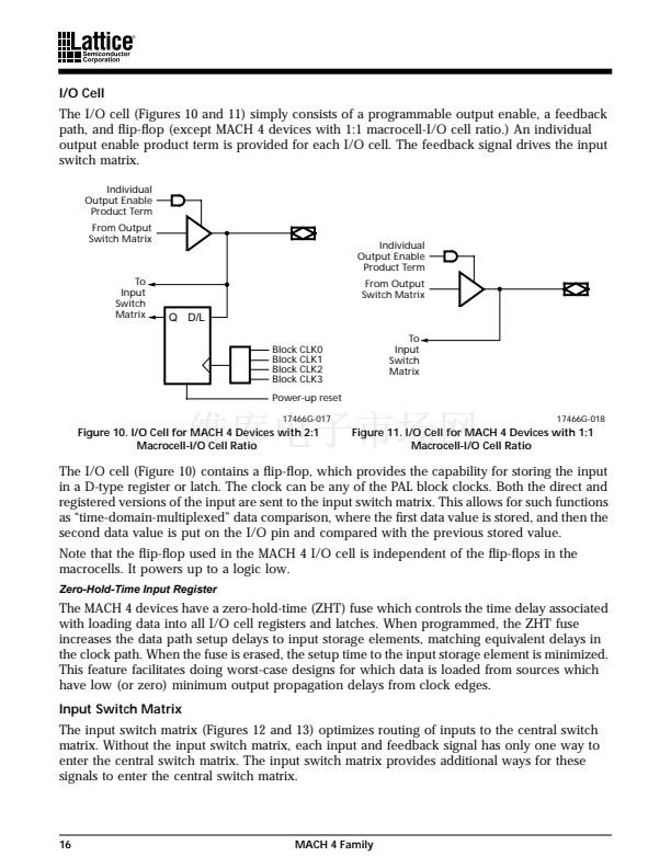
250 /10 seconds at terminals
Mechanical Data
Case:
SMA molded plastic over passivated chip
Terminals:
Solder plated solderable per
MIL-STD-750, method 2026
Polarity:
Color band denotes cathode band end
Weight:
0.004 ounce, 0.118 gram
D IM E N S IO N S
D IM
A
B
C
D
E
F
G
H
J
K
L
M
N
P
in c h e s
M in .
0 .2 1 6
0 .1 7 6
0 .0 9 4
0 .1 7 0
0 .0 3 9
0 .0 8 0
0 .0 6 8
0 .1 1 2
0 .0 5 7
-
0 .0 1 6
0 .1 0 9
0 .1 0 5
0 .0 7 8
M a x .
0 .2 2 6
0 .1 8 2
0 .1 0 0
0 .1 7 6
0 .0 5 5
0 .0 8 1
0 .0 8 3
0 .1 1 8
-
0 .0 1 8
-
0 .1 1 5
0 .1 0 7
0 .0 8 1
M in .
5 .4 8
4 .4 8
2 .4 0
4 .3 3
1 .0 0
2 .0 3
1 .7 2
2 .8 5
1 .4 4
-
0 .4 0
2 .7 7
2 .6 7
2 .0 0
m m
M a x .
5 .7 4
4 .6 3
2 .5 5
4 .4 8
1 .4 0
2 .0 7
2 .1 0
3 .0 0
-
0 .4 5
-
2 .9 3
2 .7 3
2 .0 5
N o te
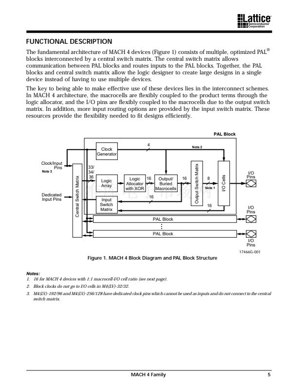
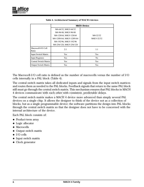
Maximum Ratings and Electrical Characteristics
Ratings at 25
ambient temperature unless otherwise specified.
Symbols
GROA
GROB
GROD
GROG
GROJ
GROK
GROM
Units
Maximum repetitive peak reverse voltage
Maximum RMS voltage
Maximum DC blocking voltage
Maximum average forward rectified current
at T
L
=100
Peak forward surge current
8.3mS single half sine-wave superimposed
on rated load (MIL-STD-750D 4066 method)
Maximum instantaneous forward voltage at 1.5A
Maximum DC reverse current
at rated DC blocking voltage
T
A
=25
T
A
=125
V
RRM
V
RMS
V
DC
I
(AV)
I
FSM
V
F
I
R
T
rr
C
J
R
R
JA
JL
50
35
50
100
70
100
200
140
200
400
280
400
1.5
50.0
1.30
5.0
200.0
600
420
600
800
560
800
1000
700
1000
Volts
Volts
Volts
Amps
Amps
Volts
A
Maximum reverse recovery time (Note 1)
Typical junction capacitance (Note 2)
Typical thermal resistance (Note 3)
Operating junction and storage temperature range
150
50.0
55.0
18.0
-55 to +150
250
500
nS
F
/W
T
J
, T
STG
Notes:
(1) Reverse recovery test conditions: I
F
=0.5A, I
R
=1.0A, I
rr
=0.25A
(2) Measured at 1.0MHz and applied reverse voltage of 4.0 volts
(3) Thermal resistance from junction to ambient and junction to lead P.C.B. mounted on 0.27X0.27聰 (7.0X7.0mm) copper pad areas
1


 1
1
 2
2
 3
3
 4
4
 5
5
 6
6
 7
7
 8
8
 9
9
 10
10
 11
11
 12
12
 13
13
 14
14
 15
15
 16
16
 17
17
 18
18
 19
19
 20
20
 21
21
 22
22
 23
23
 24
24
 25
25
 26
26
 27
27
 28
28
 29
29
 30
30
 31
31
 32
32
 33
33
 34
34
 35
35
 36
36
 37
37
 38
38
 39
39
 40
40
 41
41
 42
42
 43
43
 44
44
 45
45
 46
46
