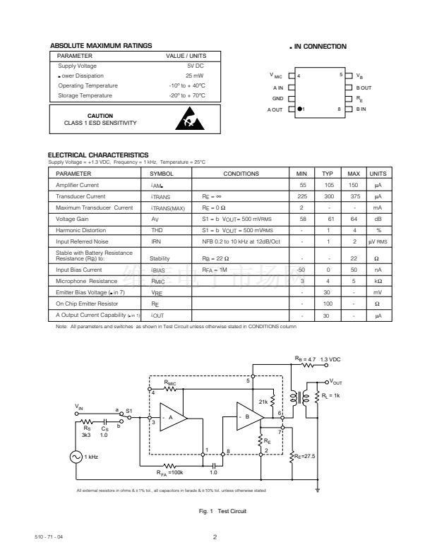
鈩?/div>
microphone decoupling resistor, on-chip
STANDARD PACKAGING
鈥?8 pin MICROpac
鈥?8 pin PLID
廬
鈥?8 pin SLT
鈥?Chip (61 x 55 mils)
DESCRIPTION
The GP509 is a Class A amplifier utilizing Gennum鈥檚 proprietary
low voltage JFET technology. It consists of a single-
ended, low noise inverting gain block, a Class A output
stage, and an on-chip microphone decoupling resistor.
Block A typically has an open loop voltage gain of 56 dB,
with the closed loop gain set by the ratio of the feedback
resistor to the source impedance. It is recommended that
the maximum closed loop gain be 20 dB lower than the
open loop gain. All blocks of the device are internally bias
compensated, preventing any DC current flow via external
feedback resistors. Without this compensation, audible
scratchiness would be present during changes in volume
control settings.
The output stage of the GP509 is a Class A current drive.
It has a fixed reference voltage of typically 30 mV at pin 7
of the device. The current that flows in the transducer is the
ratio of the 30 mV reference voltage and the on-chip emitter
resistor (R
E
). To increase the bias current in the transducer,
simply place an external R
E
resistor from pin 7 to ground,
thereby decreasing the equivalent emitter resistance and
increasing the current.
V
B
5
V
MIC
4
R
MIC
21k
3
A IN
6
-
A
-
B
7
R
E
1
A OUT
8
B IN
2
GND
B OUT
R
E
BLOCK DIAGRAM
Revision Date: January 1996
Document No. 510 - 71 - 04
GENNUM CORPORATION P.O. Box 489, Stn A, Burlington, Ontario, Canada L7R 3Y3
Japan Branch: A-302, M i yamae Vi l l age, 2鈥?0鈥?2 M i yamae, Suginami鈥搆u, Tokyo 168, Japan
tel. (905) 632-2996 fax: (905) 632-2055
tel. (03) 3247-8838
fax (03) 3247-8839


 1
1
 2
2
 3
3
 4
4
