鈩?/div>
I
D
鈥?3.6A
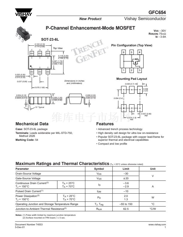
P-Channel Enhancement-Mode MOSFET
SOT-23-6L
0.122 (3.10)
0.114 (2.90)
Top View
0.118 (3.00)
0.106 (2.70)
0.067 (1.70)
0.059 (1.50)
CH
EN ET
T
REN
F
Pin Configuration (Top View)
6
5
廬
4
G
1
0.020 (0.50)
0.010 (0.25)
0.037 (0.95)
0.075 (1.90)
2
3
Dimensions in inches
and (millimeters)
Mounting Pad Layout
0.028 (0.7)
0.039
(1.07)
0.008 (0.20)
0.004 (0.10)
0.004 (0.10)
0.0005 (0.013)
0.039 (1.00)
0.036 (0.90)
0.094 (2.4)
10擄 Typical
0.037 (0.95)
Ref.
0.074 (1.9)
Ref.
Mechanical Data
Case:
SOT-23-6L package
Terminals:
Leads solderable per MIL-STD-750,
Method 2026
Marking Code:
54
Features
鈥?Advanced trench process technology
鈥?High density cell design for ultra low on-resistance
鈥?Popular SOT-23-6L package with copper lead-frame for
superior thermal and electrical capabilities
鈥?Compact and low profile
Maximum Ratings and Thermal Characteristics
(T
Parameter
Drain-Source Voltage
Gate-Source Voltage
Continuous Drain Current
(2)
T
J
= 150擄C
Pulsed Drain Current
(1)
Power Dissipation
(2)
T
J
= 150擄C
T
A
= 25擄C
T
A
= 70擄C
T
A
= 25擄C
T
A
= 70擄C
Symbol
V
DS
V
GS
I
D
I
DM
P
D
T
J
, T
stg
R
胃JA
A
= 25擄C unless otherwise noted)
Limit
鈥?0
Unit
V
鹵
20
鈥?3.6
鈥?2.9
鈥?0
2.0
1.3
鈥?5 to 150
62.5
A
W
擄C
擄C/W
Operating Junction and Storage Temperature Range
Junction-to-Ambient Thermal Resistance
(2)
Notes:
(1) Pulse width limited by maximum junction temperature
(2) Surface mounted on FR4 board, t
鈮?/div>
5 sec.
Document Number 74553
5-Dec-01
www.vishay.com
1


 1
1
 2
2
 3
3
 4
4
