622 Mbit/s
MUX/DeMUX
Chip Set
GD16131/GD16132
General Description
The GD16131, 32:4 / Quad 8:1 MUX and
the GD16132, 4:32 / Quad 1:8 DeMUX
are intended for use in 2.5 Gbit/s trans-
mission systems. The high-speed inter-
face is designed to accommodate the
requirements of the GD16554 (4:1 MUX)
and the GD16543 (1:4 DeMUX) both
meeting CCITT specifications at
2.5 Gbit/s SDH STM-16. The GD16131
and GD16162 take care of the interface
between the high-speed devices differen-
tial ECL level I/O鈥檚 at 622 Mbit/s and
lower speed CMOS gate arrays at
78 Mbit/s. Hence they are dual supply
devices shifting levels between true ECL
and TTL.
The GD16131 and GD16132 are made
as four identical blocks of 8 bit and a
clock driver circuit. The 8 bit blocks are
implemented as shift registers to obtain
the best speed/power ratio of the process
technology used. Also this means easy
clock distribution with small delay be-
tween incoming and outgoing signals.
For the GD16131 the 622 Mbit/s data
outputs are re-timed at the chip edge to
cut down delay from clock-in to data-out,
allowing counter directional clocking.
Thus the on-chip delay, except output
buffer load dependant delay, is kept be-
low 1 ns. A 622 MHz output clock with
close timing relation to the data outputs
also allows co-directional clocking. On
both MUX and DeMUX, the subdivided
78 MHz clock are also re-timed at the
chip edge to cut down delay from the
622 MHz input clock. The phase relation
between low-speed data and the subdi-
vided output clock are selectable in four
phases.
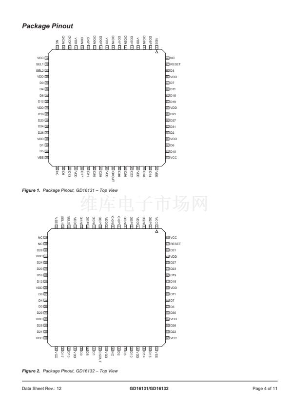
The GD16131 and GD16132 are pack-
aged in 68 pin Multi Layer Ceramic
(MLC) packages, yielding excellent high-
speed signal accommodation and ther-
mal conditions. The chip set is designed
for an operating temperature between
鈥?
擄C
and +85
擄C,
case temperature.
With power consumption of 1.3 W typical
for both GD16131 and GD16132, only
little or no heat sink is required.
Bit naming convention
Naming of pins on parallel ports is made
assuming the transfer bit order to be in-
creasing starting with position D0, D1, ...,
D31.
Features
GD16131
l
l
Quad 8:1 MUX
All high-speed I/O鈥檚 are differential,
ECL level.
All low-speed I/O鈥檚 are TTL level,
outputs drive 10 pF at 78 MHz.
Subdivided output clock to data rela-
tion selectable in four phases.
Dual supply: +5 V, -5.2 V.
68 pin MLC flat package.
High-speed pins on single side of
package for easy PCB routing.
Power consumption: 1.3 W typical.
l
l
l
l
l
l
GD16132
l
l
Quad 1:8 DeMUX
All high-speed I/O鈥檚 are differential,
ECL level.
All low-speed I/O鈥檚 are TTL level,
outputs drive 10 pF at 78 MHz.
Subdivided output clock to data
relation selectable in four phases.
Dual supply: +5 V, -5.2 V.
68 pin MLC flat package.
High-speed pins on single side of
package for easy PCB routing.
Power consumption: 1.3 W typical.
l
D0
D4
:
D24
D28
D1
D5
:
D25
D29
D2
D6
:
D26
D30
D3
D7
:
D27
D31
D0
D4
:
D24
D28
D1
D5
:
D25
D29
D2
D6
:
D26
D30
D3
D7
:
D27
D31
VEE
VDD
VCC
CKIP
CKIN
SEL1
SEL2
RESET
DO0P
DO0N
DI0P
DI0N
l
DO1P
DO1N
DI1P
DI1N
l
l
l
DO2P
DO2N
DI2P
DI2N
DO3P
DO3N
VTT
VEE
VDD
VCC
DI3P
DI3N
l
CKOP
CKON
CKIP
CKIN
SEL1
SEL2
RESET
Clock
Generator
CKOUT
Clock
Generator
CKOUT
Data Sheet Rev.: 12


 1
1
 2
2
 3
3
 4
4
 5
5
 6
6
 7
7
 8
8
 9
9
 10
10
 11
11
