HDTV
1.5 Gbit/s
Re-timer
GD14526
Preliminary
General Information
The GD14526 Re-timer is designed for
1.2 Gbit/s - 1.5 Gbit/s point-to-point serial
transmission systems such as HDTV sig-
nals according to SMPTE292. Alterna-
tively the GD14526 can be configured to
operate in the 300 Mbit/s - 375 Mbit/s
range.
The device provides a fully integrated so-
lution for Clock Recovery and Data
(CDR) Re-timing and includes an output
driver for 50/75
S
cables. The CDR can
be bypassed for data rates outside the
VCO range.
The Clock and Data Recovery circuit
consists of:
u
a Bang-Bang Phase Detector (PD)
with data re-timing
u
a Phase-Frequency Comparator
(PFC)
u
a Lock Detect Circuit (LDC) with
Lock Alarm Output
u
a Tristatable Charge Pump
u
a wide tuning range VCO.
The VCO centre frequency is determined
by the REFCK multiplied by 20. The loop
filter time constant is determined by an
external RC filter.
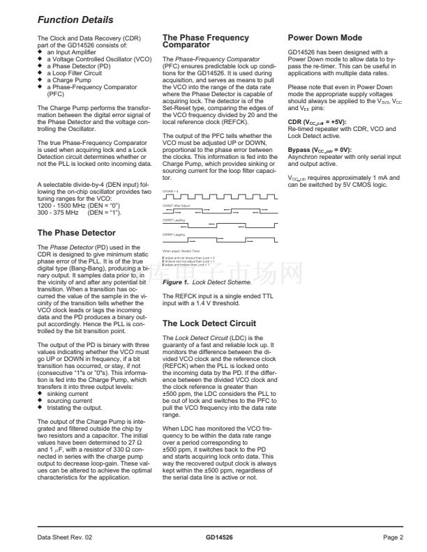
When in lock, the digital Lock Detect
Circuit (LDC) uses the incoming data to
control the PLL. When not in lock, i.e. the
VCO frequency is more than 500 ppm
away from the REFCK frequency, the
LDC switches to the local clock (REFCK)
until the VCO frequency once more en-
ters the 鹵500 ppm range. Then it
switches back to the PD, comparing the
VCO clock to the incoming data stream.
The LDC continuously monitors the VCO
frequency against the REFCK input,
clearing LOCK if the VCO leaves the lock
range.
The high-speed data input is differential
and compatible with PECL levels. It is
connected via loop-through transmission
lines to minimise stub related reflections.
The open collector cable driver has dif-
ferential outputs and the current in the
output stage can be adjusted to a maxi-
mum of 36 mA.
The GD14526 is packaged in a 40 pin
leaded Multi Layer Ceramic (MLC) pack-
age with cavity down for easy cooling.
Features
l
Two operating ranges:
鈥?/div>
鈥?/div>
1.2 -1.5 Gbit/s
300 - 375 Mbit/s
l
Jitter in accordance with SMPTE292.
l
High-speed data input and output use
Loop-through bondings to reduce
reflections.
and Lock Acquisition on one IC.
鈥?/div>
鈥?/div>
鈥?/div>
鈥?/div>
l
Complete Clock/20, Data Recovery,
l
Digitally controlled capture and lock.
Full capture range with true
Phase/Frequency detect between
VCO-CLK and REFCK.
Bang-Bang Phase Detector
between VCO-CLK and DATA.
Lock in range 鹵500 ppm or
鹵2000 ppm referred to REFCK.
Lock Alarm Output.
l
Re-timed differential 50/75
S
cable
l
Supply operation: 5 V and 3.3 V.
l
Power dissipation: 1100 mW typ.
l
Power down mode for bypass
operation.
driver output with external termination
resistors.
SIP
SIN
DEN
VCO
DI
SOP
SON
CIP
VCC_CDR
Div.
/4
Bang
Bang
Phase
Detector
DO
U
D
l
40 pin Multi Layer Ceramic (MLC)
leaded package with transmission
lines.
VEE
V3V3
V3V3A
VCCA
VCCD
VCCO
OUTCHP
VCTL
Applications
l
HDTV Studio equipment.
l
Gigabit Ethernet
/20
Clock
Divide
Lock
Detect
V
R
PFC
U
D
4:2
MUX
U
D
Charge
Pump
Data Sheet Rev. 02
SEL0
SEL1
REFCK
LOCK
CKOUT


 1
1
 2
2
 3
3
 4
4
 5
5
 6
6
 7
7
 8
8
