鈥?/div>
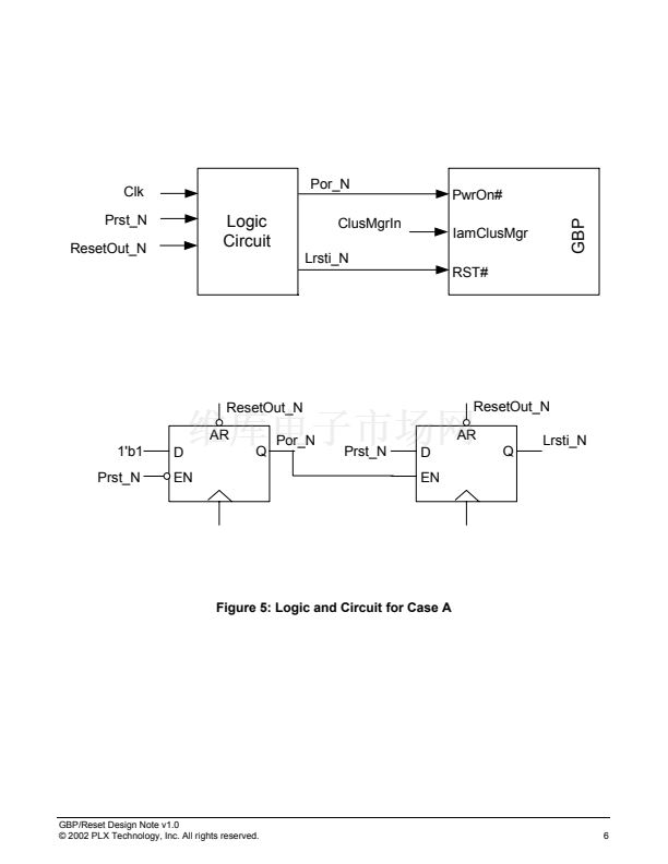
Section 4 lists the signals used in our sample circuit.
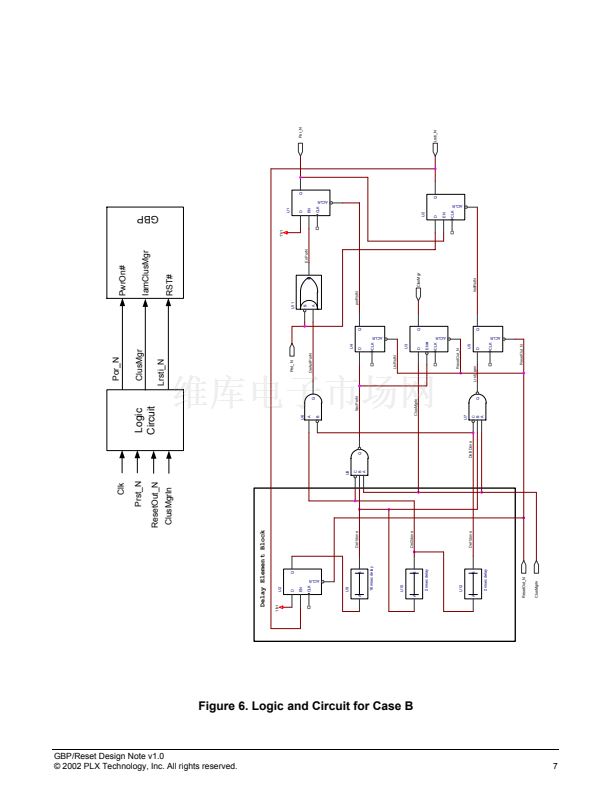
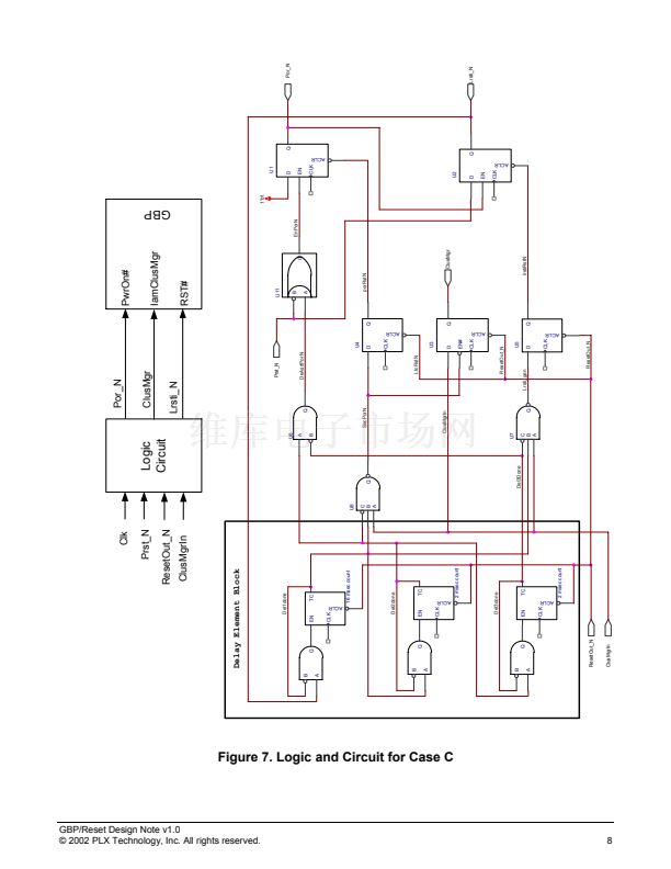
Section 5 describes the Primary Node operation and sample circuit.
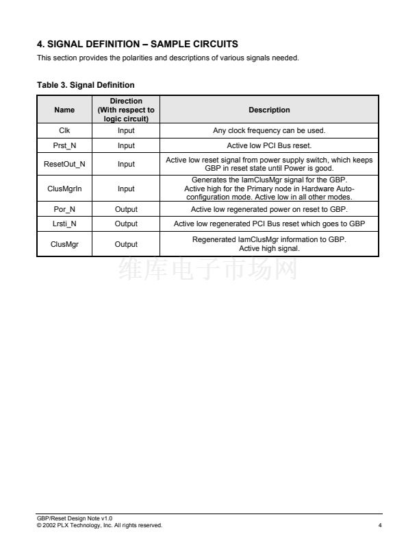
Section 6 describes the Secondary Node operation and sample circuit.
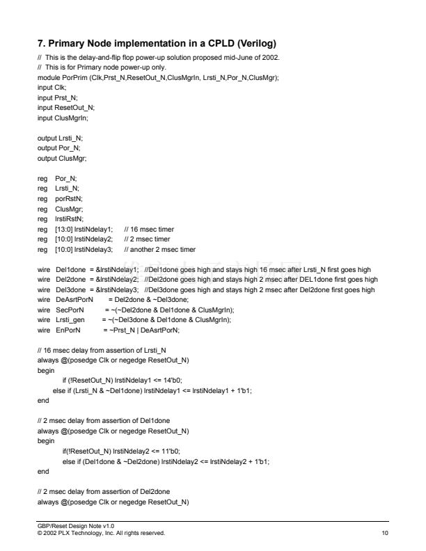
Section 7 provides the Verilog code for the Primary Node sample circuit.
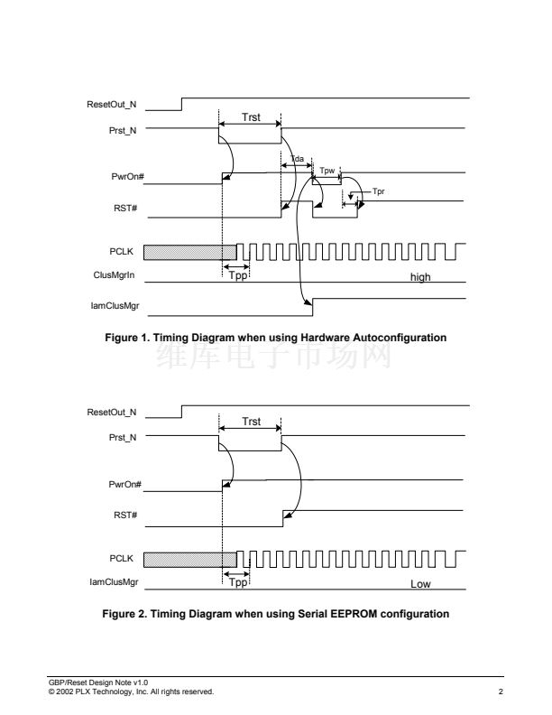
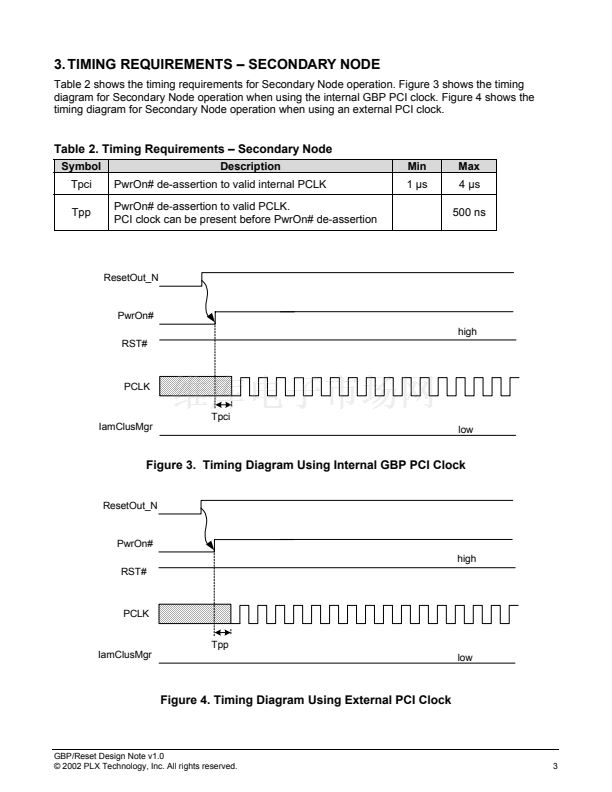
2. TIMING REQUIREMENTS 鈥?PRIMARY NODE
Table 1 shows the timing requirements for Primary Node operation. Figure 1 shows the timing diagram
for Primary Node operation when using Hardware Autoconfiguration. Figure 2 shows the timing
diagram for Primary Node operation when using Serial EEPROM configuration.
Table 1. Timing Requirements 鈥?Primary Node
Symbol
Tpp
Tda
Tpw
Trst
Tpr
Description
PwrOn# de-assertion to valid PCLK.
PCI clock can be present before PwrOn# de-assertion
RST# de-assertion to PwrOn# re-assertion
Second power-on-reset assertion width
Reset active time after power stable
PwrOn# de-assertion to RST# de-assertion
RST# final de-assertion to initial configuration to GBP device
Min
Max
500 ns
16 ms
1 ms
1 ms
15 碌s
32 ms
* Note: In the timing diagrams in Figures 1 and 2, the assertions and de-assertions of the signals specified
are not with respect to the PCLK signal.
錚?/div>
PLX Technology, Inc., 2002
PLX Technology, Inc, 870 Maude Avenue, Sunnyvale, CA 94085, Phone 408-774-9060, Fax 408-774-2169
Products and Company names are trademarks/registered trademarks of their respective holders.


 1
1
 2
2
 3
3
 4
4
 5
5
 6
6
 7
7
 8
8
 9
9
 10
10
 11
11
 12
12
