convenient 8 pin SIP packaging.
鈥?/div>
both can be configured as a gain stage with reduced
bandwidth.
DESCRIPTION
The GB4550 and GB4550A are high performance mono-
lithic video buffer/clamps made on Gennum's LSI process.
They feature a wideband differential amplifier that can be
configured as a gain stage. The output signal voltage is
limited to +2V above the clamp level in order to prevent
damage to crosspoints connected to the output.
The clamping level can be set for normal sync tip clamping
by connecting pin 4 to -0.286 volts. For other applications,
the clamping voltage level can be varied from -5.5 to +5.5
volts.
The GB4550A features a tight delay spread of only
鹵
0.15
degrees while the GB4550 maintains a
鹵
1.5 degree delay
spread. Both devices operate from
鹵
9 to
鹵
12 V power
supplies and will directly interface with Gennum's video
crosspoint switches.
The 8 pin SIP package is ideally suited for space restricted
board layouts.
GB4550 and GB4550A
APPLICATIONS
鈥?/div>
Input buffering and clamping to crosspoint switches
1
2
3
4
5
6
7
8
鈥?/div>
Inter - system video signal clamping
PIN CONNECTIONS
Pin No.
1
2
3
4
5
6
7
8
GB4550
+IN
V
CC
COMP
V
CL
C
X
V
EE
-IN
OUT
GB4550A
+IN
V
CC
NC
V
CL
C
X
V
EE
-IN
OUT
Function
non-inverting input
positive power supply
frequency compensation or NC
clamp voltage input
external capacitor
negative power supply
inverting input
output
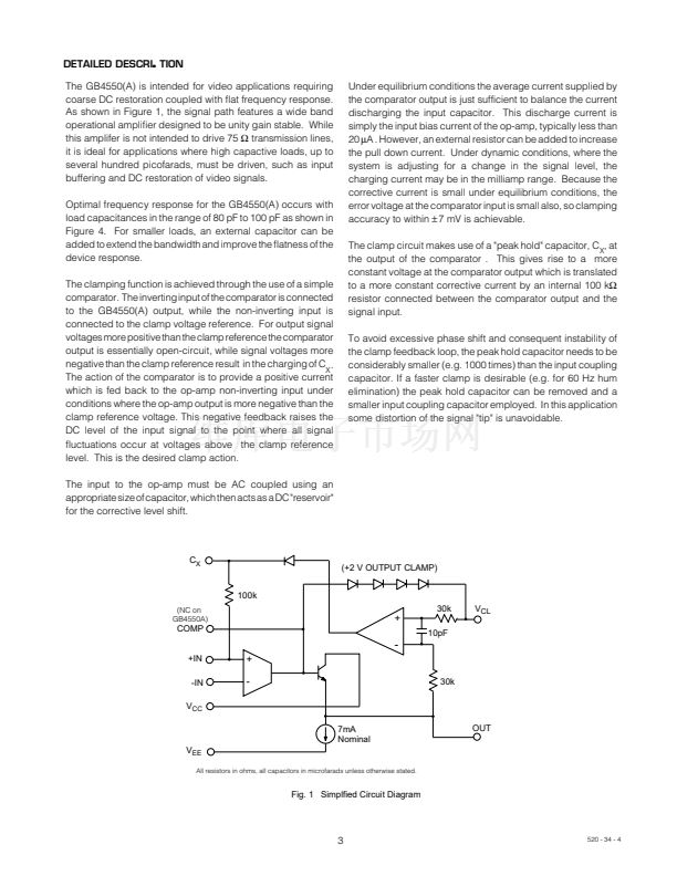
C
X
(+2 V OUTPUT CLAMP)
100k
(NC on
GB4550A)
30k
+
10pF
V
CL
COMP
-
+IN
-IN
V
CC
7mA
Nominal
V
EE
OUT
+
-
30k
ORDERING INFORMATION
Part Number
GB4550 - CSA
GB4550ACSA
Package Type
8 pin SIP
8 pin SIP
Temperature Range
0 to 70 C
0 to 70 C
o
o
All resistors in ohms, all capacitors in microfarads unless otherwise stated
SIMPLIFIED CIRCUIT DIAGRAM
Revision Date: February 1994
Document No. 520 - 34 - 4
GENNUM CORPORATION P.O. Box 489, Stn A, Burlington, Ontario, Canada L7R 3Y3 tel. (905) 632-2996 fax: (905) 632-5946
Japan Branch: A-302, Miyamae Village, 2-10-42 Miyamae, Suginami-ku, Tokyo 168, Japan
tel. (03) 3334-7700
fax: (03) 3247-8839


 1
1
 2
2
 3
3
 4
4
 5
5
