鈥?7A, -200V, RDS(on) = 0.735鈩?/div>
鈥?Second Generation Rad Hard MOSFET Results From New Design Concepts
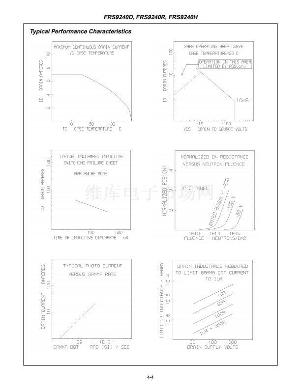
鈥?Gamma
-
-
-
-
-
Meets Pre-Rad Speci鏗乧ations to 100KRAD(Si)
De鏗乶ed End Point Specs at 300KRAD(Si) and 1000KRAD(Si)
Performance Permits Limited Use to 3000KRAD(Si)
Survives 3E9RAD(Si)/sec at 80% BVDSS Typically
Survives 2E12 Typically If Current Limited to IDM
鈥?Gamma Dot
鈥?Photo Current
鈥?Neutron
S
G
D
- 5.0nA Per-RAD(Si)/sec Typically
- Pre-RAD Speci鏗乧ations for 1E13 Neutrons/cm
2
- Usable to 1E14 Neutrons/cm
2
Description
Intersil has designed a series of SECOND GENERATION hardened power MOS-
FETs of both N and P channel enhancement types with ratings from 100V to 500V,
1A to 60A, and on resistance as low as 25m鈩? Total dose hardness is offered at
100K RAD(Si) and 1000KRAD(Si) with neutron hardness ranging from 1E13n/cm
2
for 500V product to 1E14n/cm
2
for 100V product. Dose rate hardness (GAMMA
DOT) exists for rates to 1E9 without current limiting and 2E12 with current limiting.
This MOSFET is an enhancement-mode silicon-gate power 鏗乪ld- effect transistor
of the vertical DMOS (VDMOS) structure. It is specially designed and processed to
exhibit minimal characteristic changes to total dose (GAMMA) and neutron (n
o
)
exposures. Design and processing efforts are also directed to enhance survival to
heavy ion (SEU) and/or dose rate (GAMMA DOT) exposure.
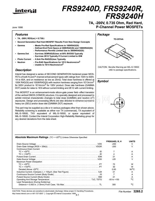
This part may be supplied as a die or in various packages other than shown above.
Reliability screening is available as either non TX (commercial), TX equivalent of
MIL-S-19500, TXV equivalent of MIL-S-19500, or space equivalent of
MIL-S-19500. Contact the Intersil Corporation High-Reliability Marketing group for
any desired deviations from the data sheet.
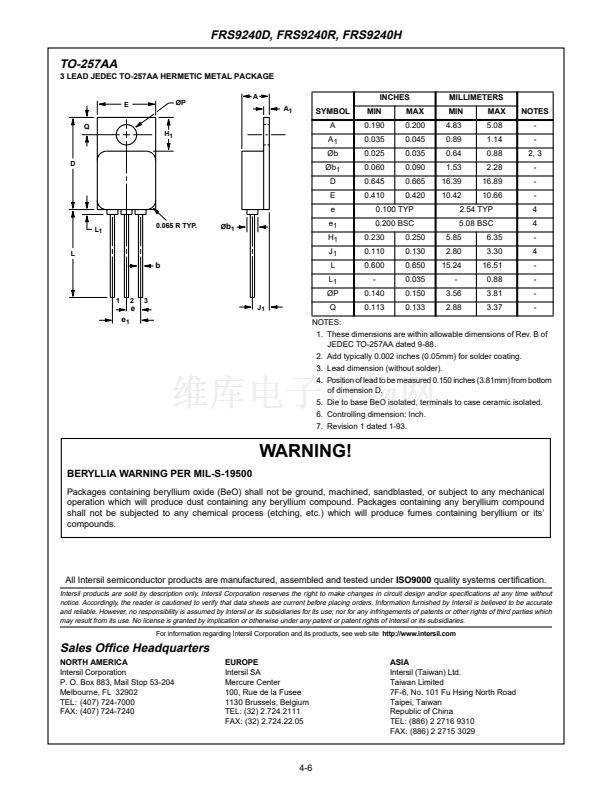
CAUTION: Beryllia Warning per MIL-S-19500
refer to package speci鏗乧ations.
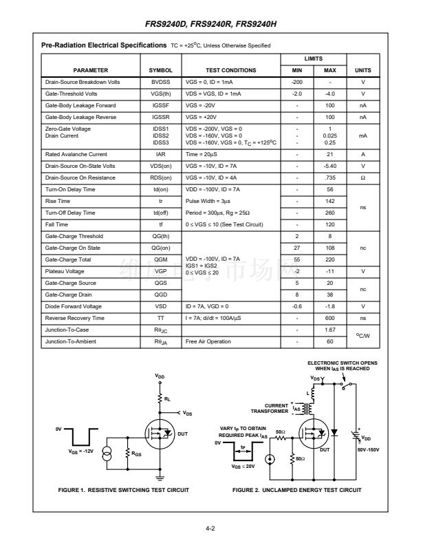
Symbol
D
G
S
Absolute Maximum Ratings
(TC = +25
o
C) Unless Otherwise Speci鏗乪d
FRS9240D, R, H
-200
-200
7
4
21
鹵20
75
30
0.60
21
7
21
-55 to +150
300
UNITS
V
V
A
A
A
V
W
W
W/
o
C
A
A
A
o
C
o
C
Drain-Source Voltage. . . . . . . . . . . . . . . . . . . . . . . . . . . . . . . . . . . . . . . . . . . . . . . . . . . . . . . VDS
Drain-Gate Voltage (RGS = 20k鈩?. . . . . . . . . . . . . . . . . . . . . . . . . . . . . . . . . . . . . . . . . . . VDGR
Continuous Drain Current
TC = +25
o
C . . . . . . . . . . . . . . . . . . . . . . . . . . . . . . . . . . . . . . . . . . . . . . . . . . . . . . . . . . . . . .ID
TC = +100
o
C . . . . . . . . . . . . . . . . . . . . . . . . . . . . . . . . . . . . . . . . . . . . . . . . . . . . . . . . . . . . .ID
Pulsed Drain Current . . . . . . . . . . . . . . . . . . . . . . . . . . . . . . . . . . . . . . . . . . . . . . . . . . . . . . . IDM
Gate-Source Voltage . . . . . . . . . . . . . . . . . . . . . . . . . . . . . . . . . . . . . . . . . . . . . . . . . . . . . . .VGS
Maximum Power Dissipation
TC = +25
o
C . . . . . . . . . . . . . . . . . . . . . . . . . . . . . . . . . . . . . . . . . . . . . . . . . . . . . . . . . . . . . PT
TC = +100
o
C . . . . . . . . . . . . . . . . . . . . . . . . . . . . . . . . . . . . . . . . . . . . . . . . . . . . . . . . . . . . PT
Derated Above +25
o
C . . . . . . . . . . . . . . . . . . . . . . . . . . . . . . . . . . . . . . . . . . . . . . . . . . . . . . .
Inductive Current, Clamped, L = 100碌H, (See Test Figure). . . . . . . . . . . . . . . . . . . . . . . . . . ILM
Continuous Source Current (Body Diode) . . . . . . . . . . . . . . . . . . . . . . . . . . . . . . . . . . . . . . . . . IS
Pulsed Source Current (Body Diode) . . . . . . . . . . . . . . . . . . . . . . . . . . . . . . . . . . . . . . . . . . ISM
Operating And Storage Temperature . . . . . . . . . . . . . . . . . . . . . . . . . . . . . . . . . . . . . TJC, TSTG
Lead Temperature (During Soldering)
Distance > 0.063 in. (1.6mm) From Case, 10s Max. . . . . . . . . . . . . . . . . . . . . . . . . . . . . . . TL
CAUTION: These devices are sensitive to electrostatic discharge; follow proper IC Handling Procedures.
http://www.intersil.com or 407-727-9207
|
Copyright
漏
Intersil Corporation 1999
File Number
3265.2
4-1


 1
1
 2
2
 3
3
 4
4
 5
5
 6
6
