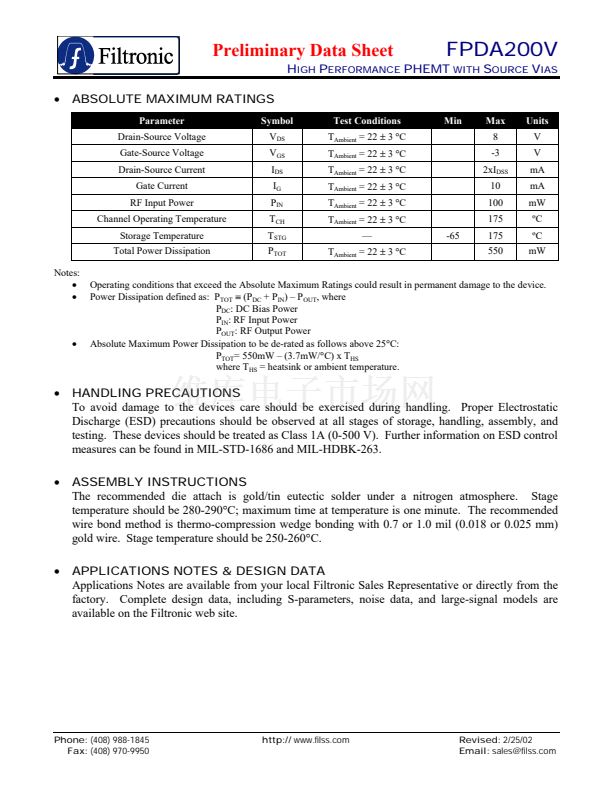
鈥?/div>
DESCRIPTION AND APPLICATIONS
The FPDA200V is an Aluminum Gallium Arsenide / Indium Gallium Arsenide (AlGaAs/InGaAs)
Pseudomorphic High Electron Mobility Transistor (PHEMT), utilizing an Electron-Beam direct-
write 0.25
碌m
by 200
碌m
Schottky barrier gate. The recessed 鈥渕ushroom鈥?gate structure minimizes
parasitic gate-source and gate resistances. The epitaxial structure and processing have been
optimized for high dynamic range.
Typical applications include high dynamic range driver stages for commercial applications including
wireless infrastructure systems, broad bandwidth amplifiers, and optical systems.
Source vias have been added for improved performance and assembly convenience. Each via hole
has 0.02 nH of inductance. Additionally, the via holes remove the need for source bond wires,
meaning only two bond wires are required for assembly. Because the via connects the source pad to
the backside metallization, self-bias configurations should be designed with caution.
鈥?/div>
ELECTRICAL SPECIFICATIONS @ T
Ambient
= 25擄C
Parameter
Saturated Drain-Source Current
Power at 1-dB Compression
Power Gain at 1-dB Compression
Power-Added Efficiency
Maximum Drain-Source Current
Transconductance
Gate-Source Leakage Current
Pinch-Off Voltage
Gate-Source Breakdown
Voltage Magnitude
Gate-Drain Breakdown
Voltage Magnitude
Thermal Resistivity
frequency=18 GHz
Symbol
I
DSS
P-1dB
G-1dB
PAE
I
MAX
G
M
I
GSO
V
P
|V
BDGS
|
|V
BDGD
|
螛
JC
Test Conditions
V
DS
= 2 V; V
GS
= 0 V
V
DS
= 5 V; I
DS
= 50% I
DSS
V
DS
= 5 V; I
DS
= 50% I
DSS
V
DS
= 5 V; I
DS
= 50% I
DSS
V
DS
= 2 V; V
GS
= 1 V
V
DS
= 2 V; V
GS
= 0 V
V
GS
= -5 V
V
DS
= 2 V; I
DS
= 1 mA
I
GS
= 1 mA
I
GD
= 1 mA
-0.25
6
8
50
Min
40
19
11
Typ
60
21
12.5
55
125
70
1
-0.8
7
9
260
10
-1.5
Max
85
Units
mA
dBm
dB
%
mA
mS
碌A
V
V
V
擄C/W
Phone:
(408) 988-1845
Fax:
(408) 970-9950
http://
www.filss.com
Revised:
2/25/02
Email:
sales@filss.com


 1
1
 2
2
 3
3
