Mobility Transistor (pHEMT). It utilizes a 0.25
photolithography.
.
is also available in die form .
Typical applications include gain blocks and medium power stages for applications to 22 GHz.
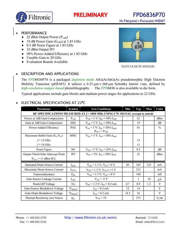
鈥?/div>
ELECTRICAL SPECIFICATIONS AT 22擄C
Parameter
Power at 1dB Gain Compression
Gain at 1dB Gain Compression
Power-Added Efficiency
Maximum Stable Gain (S
21
/S
12
)
f
= 12 GHz
f
= 18 GHz
Noise Figure
Output Third-Order Intercept Point
P
OUT
= 11 dBm SCL
Saturated Drain-Source Current
Maximum Drain-Source Current
Transconductance
Gate-Source Leakage Current
Pinch-Off Voltage
Gate-Source Breakdown Voltage
Gate-Drain Breakdown Voltage
Thermal Resistivity (see Notes)
I
DSS
I
MAX
G
M
I
GSO
|V
P
|
|V
BDGS
|
|V
BDGD
|
胃
JC
V
DS
= 1.3 V; V
GS
= 0 V
V
DS
= 1.3 V; V
GS
鈮?/div>
+1 V
V
DS
= 1.3 V; V
GS
= 0 V
V
GS
= -5 V
V
DS
= 1.3 V; I
DS
= 0.2 mA
I
GS
= 0.2 mA
I
GD
= 0.2 mA
V
DS
> 3V
0.7
12
14.5
85
105
215
140
1
0.9
14
16
275
10
1.3
125
mA
mA
mS
碌A(chǔ)
V
V
V
擄C/W
NF
IP3
V
DS
= 5 V; I
DS
= 25% I
DSS
V
DS
= 5V; I
DS
= 50% I
DSS
Symbol
P
1dB
SSG
PAE
MSG
Test Conditions
V
DS
= 5 V; I
DS
= 50% I
DSS
V
DS
= 5 V; I
DS
= 50% I
DSS
V
DS
= 5 V; I
DS
= 50% I
DSS
;
P
OUT
= P
1dB
V
DS
= 5 V; I
DS
= 50% I
DSS
13
11
0.5
32
dB
dBm
Min
Typ
22
19
45
Max
Units
dBm
dB
%
RF SPECIFICATIONS MEASURED AT
f
= 1850 MHz USING CW SIGNAL (except as noted)
Phone:
+1 408 850-5790
Fax:
+1 408 850-5766
http://www.filtronic.co.uk/semis
Revised:
7/15/05
Email:
sales@filcsi.com


 1
1
 2
2
 3
3
