鈥?/div>
Mobile Infrastructure
CATV / DBS
W-LAN / ISM
RFID
Defense / Homeland Security
Fixed Wireless
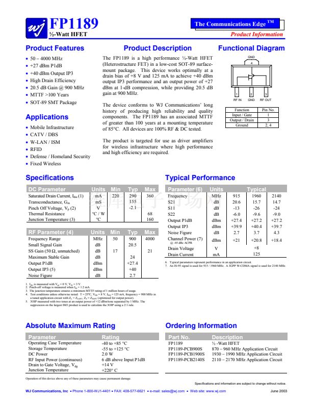
Function
Input / Gate
Output / Drain
Ground
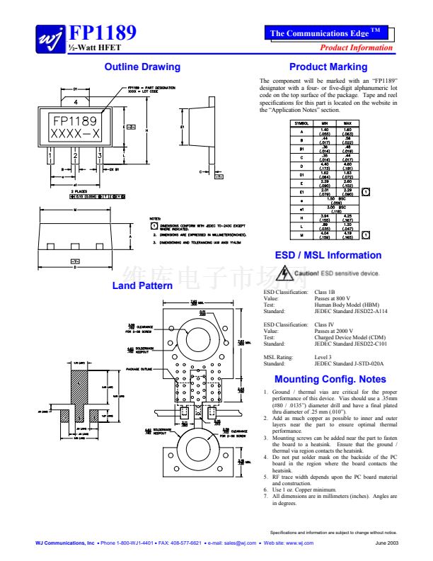
Pin No.
1
3
2, 4
Specifications
DC Parameter
Saturated Drain Current, I
dss
(1)
Transconductance, G
m
Pinch Off Voltage, V
p
(2)
Thermal Resistance
Junction Temperature (3)
Typical Performance
Units Min
mA
mS
V
擄C
/ W
擄C
220
Typ
290
155
-2.1
Max
360
Parameter (6)
Frequency
S21
S11
S22
Output P1dB
Output IP3
Noise Figure
Channel Power (7)
@ -45 dBc ACPR
Units
MHz
dB
dB
dB
dBm
dBm
dB
dBm
V
mA
915
20.6
-13
-6.0
+27.4
+39.9
2.7
+21
Typical
1960
15.7
-26
-9.6
+27.2
+40.4
3.7
+20.8
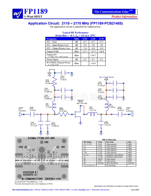
+8
125
2140
14.7
-24
-9.0
+27.2
+39.7
4.3
+18.4
68
160
RF Parameter (4)
Frequency Range
Small Signal Gain
SS Gain (50
鈩?
unmatched)
Maximum Stable Gain
Output P1dB
Output IP3 (5)
Noise Figure
1.
2.
3.
4.
Units Min
MHz
dB
dB
dB
dBm
dBm
dB
50
17
Typ
900
20.5
24
+27.4
+40
2.7
Max
4000
21
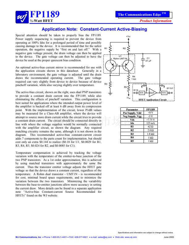
Drain Voltage
Drain Current
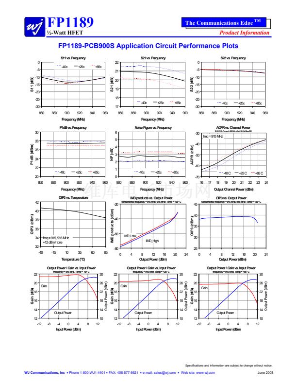
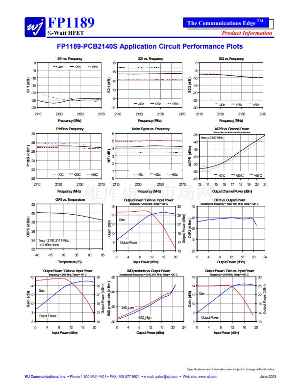
6. Typical parameters represent performance in an application circuit.
7. An IS-95 signal is used for 915 / 1960 MHz. A 3GPP W-CDMA signal is used for 2140 MHz.
I
dss
is measured with V
gs
= 0 V, V
ds
= 3 V.
Pinch-off voltage is measured when I
ds
= 1.2 mA.
The junction temperature ensures a minimum MTTF rating of 1 million hours of usage.
Test conditions unless otherwise noted: T = 25潞C, V
DS
= 8 V, I
DQ
= 125 mA, frequency = 900 MHz in
a tuned application circuit with Z
L
= Z
LOPT
, Z
S
= Z
SOPT
(optimized for output power).
5. 3OIP measured with two tones at an output power of +12 dBm/tone separated by 1 MHz. The
suppression on the largest IM3 product is used to calculate the 3OIP using a 2:1 rule.
Absolute Maximum Rating
Parameter
Operating Case Temperature
Storage Temperature
DC Power
RF Input Power (continuous)
Drain to Gate Voltage, V
dg
Junction Temperature
-40 to +85
擄C
-55 to +125
擄C
2.0 W
6 dB above Input P1dB
+14 V
+220擄 C
Ordering Information
Part No.
FP1189
FP1189-PCB900S
FP1189-PCB1900S
FP1189-PCB2140S
Rating
Description
錕?frac12; -Watt HFET
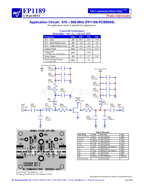
870 鈥?960 MHz Application Circuit
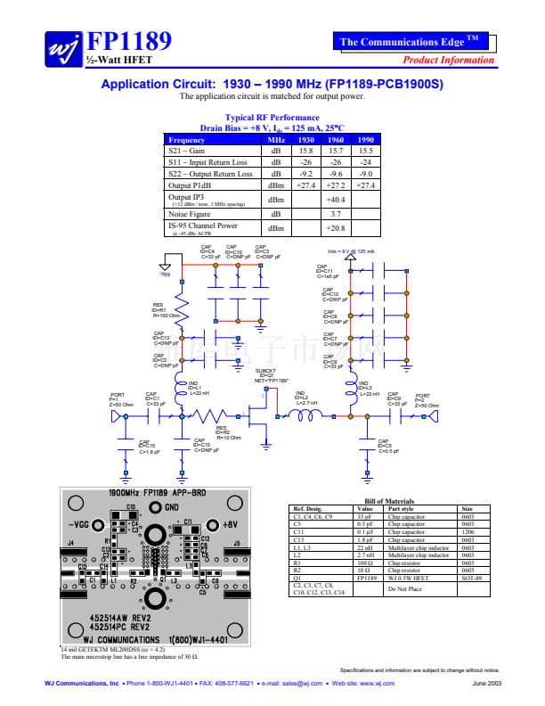
1930 鈥?1990 MHz Application Circuit
2110 鈥?2170 MHz Application Circuit
Operation of this device above any of these parameters may cause permanent damage.
Specifications and information are subject to change without notice.
WJ Communications, Inc
鈥?/div>
Phone 1-800-WJ1-4401
鈥?/div>
FAX: 408-577-6621
鈥?/div>
e-mail: sales@wj.com
鈥?/div>
Web site: www.wj.com
June 2003


 1
1
 2
2
 3
3
 4
4
 5
5
 6
6
 7
7
 8
8
 9
9
 10
10
