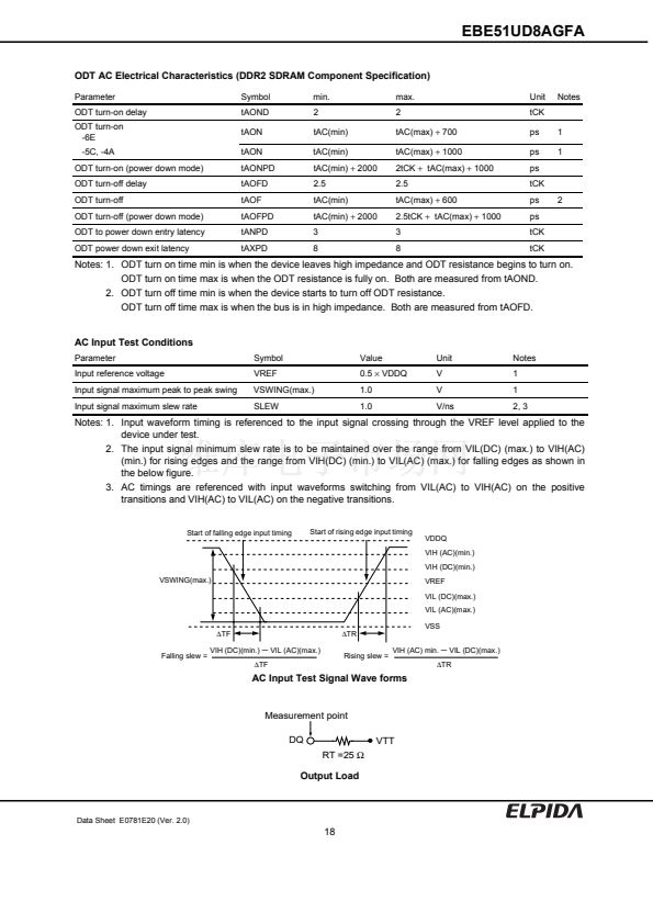
錚?/div>
)
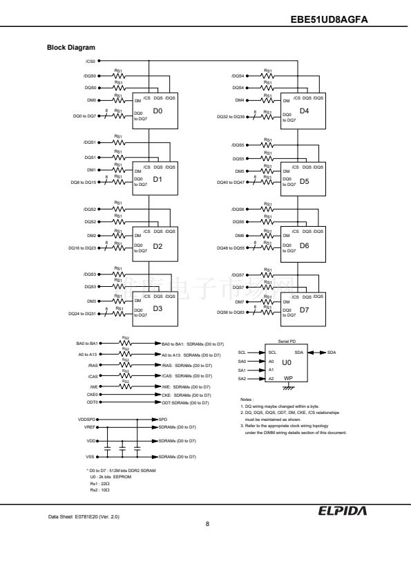
package. Read and write operations are performed at
the cross points of the CK and the /CK. This high-
speed data transfer is realized by the 4 bits prefetch-
pipelined architecture. Data strobe (DQS and /DQS)
both for read and write are available for high speed and
reliable data bus design. By setting extended mode
register, the on-chip Delay Locked Loop (DLL) can be
set enable or disable. This module provides high
density mounting without utilizing surface mount
technology.
Decoupling capacitors are mounted
beside each FBGA (碌BGA) on the module board.
Note: Do not push the components or drop the
modules in order to avoid mechanical defects,
which may result in electrical defects.
Features
鈥?/div>
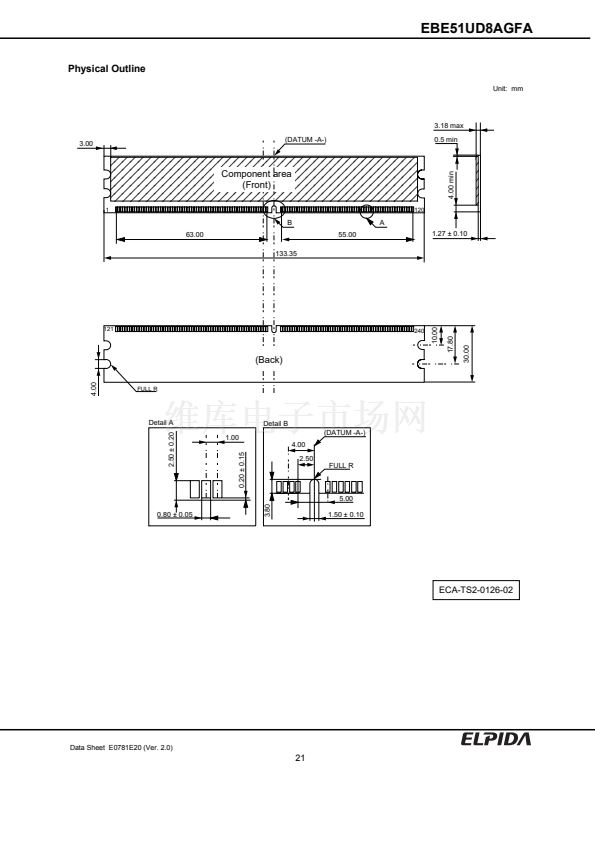
240-pin socket type dual in line memory module
(DIMM)
錚?/div>
PCB height: 30.0mm
錚?/div>
Lead pitch: 1.0mm
錚?/div>
Lead-free (RoHS compliant)
鈥?/div>
Power supply: VDD
=
1.8V
鹵
0.1V
鈥?/div>
Data rate: 667Mbps/533Mbps/400Mbps (max.)
鈥?/div>
SSTL_18 compatible I/O
鈥?/div>
Double-data-rate architecture: two data transfers per
clock cycle
鈥?/div>
Bi-directional, differential data strobe (DQS and
/DQS) is transmitted/received with data, to be used in
capturing data at the receiver
鈥?/div>
DQS is edge aligned with data for READs: center-
aligned with data for WRITEs
鈥?/div>
Differential clock inputs (CK and /CK)


 1
1
 2
2
 3
3
 4
4
 5
5
 6
6
 7
7
 8
8
 9
9
 10
10
 11
11
 12
12
 13
13
 14
14
 15
15
 16
16
 17
17
 18
18
 19
19
 20
20
 21
21
 22
22
 23
23
