DS26101
8-Port TDM-to-ATM PHY
www.maxim-ic.com
GENERAL DESCRIPTION
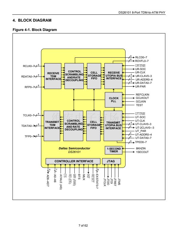
On the transmit side, the DS26101 receives ATM cells
from an ATM device through a UTOPIA II interface,
provides cell buffering (up to 4 cells), HEC generation
and insertion, cell scrambling, and converts the data
to a serial stream appropriate for interfacing to a
T1/E1 framer or transceiver. On the receive side, the
DS26101 receives a TDM stream from a T1/E1 framer
or transceiver; searches for the cell alignment; verifies
the HEC; provides cell filtering, descrambling, and cell
buffering; and passes the cells to an ATM device
through the UTOPIA II interface. Other low-level traffic
management functions are selectable for the transmit
and receive paths. The DS26101 can also be used in
fractional T1/E1 applications.
The DS26101 maps ATM cells to T1/E1 TDM frames
as specified in ATM Forum Specifications af-phy-
0016.000 and af-phy-0064.000. In the receive
direction, the cell delineation mechanism used for
finding ATM cell boundary within T1/E1 frame is
performed as per ITU I.432. The DS26101 provides a
mapping solution for up to 8 T1/E1 TDM ports. The
terms physical layer (PHY) and line side are used
synonymously in this document and refer to the
device interfacing with the line side of the DS26101.
The terms ATM layer and system side are used
synonymously and refer to the DS26101鈥檚 UTOPIA II
interface.
FEATURES
摟
摟
摟
摟
摟
摟
摟
摟
摟
摟
摟
摟
摟
摟
摟
摟
摟
摟
Supports 8 T1/E1 TDM Ports
Supports Fractional T1/E1
Compliant to ATM Forum Specifications for ATM
Over T1 and E1
Standard UTOPIA II Interface to the ATM Layer
Configurable UTOPIA Address Range
Configurable Tx FIFO Depth to 2, 3, or 4 Cells
Optional Payload Scrambling in Transmit
Direction and Descrambling in Receive Direction
per ITU I.432
Optional HEC Insertion in Transmit Direction with
Programmable COSET Polynomial Addition
HEC-Based Cell Delineation
Single-Bit HEC Error Correction in the Receive
Direction
Receive HEC-Errored Cell Filtering
Receive Idle/Unassigned Cell Filtering
User-Definable Cell Filtering
8-Bit Mux/Nonmux, Motorola/Intel Microprocessor
Interface
Internal Clock Generator Eliminates External
High-Speed Clocks
Internal One-Second Timer
Detects/Reports Up to Eight External Status
Signals with Interrupt Support
IEEE 1149.1 JTAG Boundary Scan Support
17mm x 17mm, 256-pin CSBGA
摟
FUNCTIONAL DIAGRAM
APPLICATIONS
DSLAMS
ATM Over T1/E1
Routers
IMA
8 TDM
PORTS
Dallas
Semiconductor
ORDERING INFORMATION
UTOPIA II
PART
DS26101
TEMP RANGE
-40擄C to +85擄C
PIN-PACKAGE
256 CSBGA
DS26101
Note:
Some revisions of this device may incorporate deviations from published specifications known as errata. Multiple revisions of any device
may be simultaneously available through various sales channels. For information about device errata, click here:
www.maxim-ic.com/errata.
1 of 62
REV: 032503


 1
1
 2
2
 3
3
 4
4
 5
5
 6
6
 7
7
 8
8
 9
9
 10
10
 11
11
 12
12
 13
13
 14
14
 15
15
 16
16
 17
17
 18
18
 19
19
 20
20
 21
21
 22
22
 23
23
 24
24
 25
25
 26
26
 27
27
 28
28
 29
29
 30
30
 31
31
 32
32
 33
33
 34
34
 35
35
 36
36
 37
37
 38
38
 39
39
 40
40
 41
41
 42
42
 43
43
 44
44
 45
45
 46
46
 47
47
 48
48
 49
49
 50
50
 51
51
 52
52
 53
53
 54
54
 55
55
 56
56
 57
57
 58
58
 59
59
 60
60
 61
61
 62
62
