廬
DPS9245EB
Evaluation Board
User鈥檚 Guide
Contents
1
2
3
Introduction
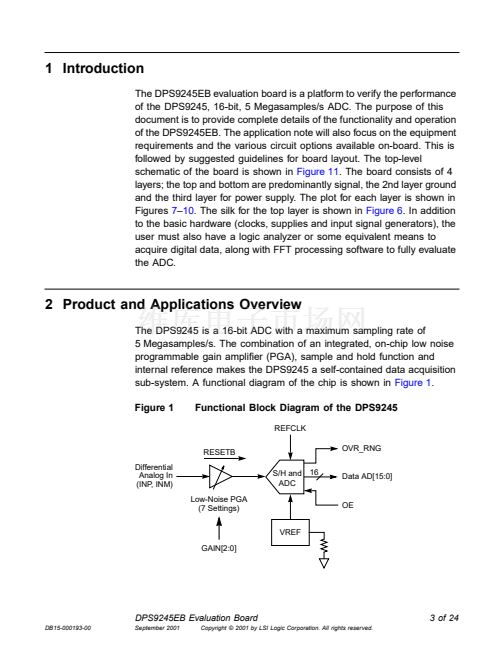
Product and Applications Overview
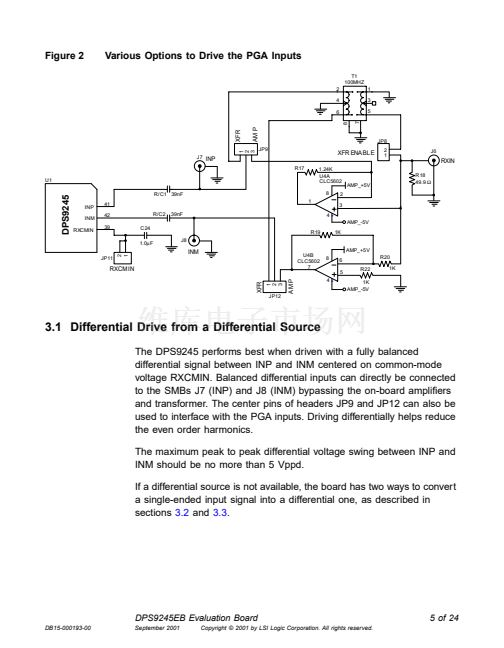
Driving the Analog Inputs
3.1
Differential Drive from a Differential Source
3.2
Single-Ended to Differential Con鏗乬uration (Using
Ampli鏗乪rs)
3.3
Single-Ended to Differential Con鏗乬uration
(Transformer Coupled)
3.4
True Single-Ended Operation of the DPS9245
3.5
Suggested External Signal Sources and Signal
Conditioning Techniques
Programmable Gain Ampli鏗乪r (PGA) Gain Control
Clock
5.1
DC-Coupling the Clock
5.2
AC-Coupling the Clock
16-Bit Parallel ADC Outputs
Various Digital Inputs/Outputs
7.1
OE
7.2
OVR_RNG
7.3
RESETB
7.4
BUSYB
Power Supplies
References, Bandgap and Common-Mode Voltage
9.1
ADC References
9.2
Bandgap/External Bias Capacitor and Resistor
9.3
The Common-Mode Voltage RXCMIN
Initializing the DPS9245EB Board
Layout Guidelines
11.1
Layers
3
3
4
5
6
7
7
7
8
9
9
9
10
10
10
10
10
11
11
12
13
13
13
14
15
15
4
5
6
7
8
9
10
11
DB15-000193-00
September 2001
Copyright 漏 2001 by LSI Logic Corporation. All rights reserved.
1 of 24


 1
1
 2
2
 3
3
 4
4
 5
5
 6
6
 7
7
 8
8
 9
9
 10
10
 11
11
 12
12
 13
13
 14
14
 15
15
 16
16
 17
17
 18
18
 19
19
 20
20
 21
21
 22
22
 23
23
 24
24
