DP83290EB FDDI Physical Layer Evaluation Board
April 1990
DP83290EB
FDDI Physical Layer Evaluation Board
1 0 Introduction
This document is intended to provide the user with an over-
view concerning the design operation and installation of
the National Semiconductor DP83290EB FDDI Physical
Layer Evaluation Board hereafter referred to as the Link
Card
Appendix A 1 is included in this document All other append-
ices can be found in the DP83290EB FDDI Physical Layer
Evaluation Board User鈥檚 Guide They are listed here for ref-
erence only
Table of Contents
1 0 INTRODUCTION
2 0 EVALUATION BOARDS AND ENVIRONMENT
2 1 Link Card Description
2 2 Link Card Features
2 3 BMAC Card Description
2 4 Station Environment (PC-AT Platform)
3 0 SYSTEM DESCRIPTION
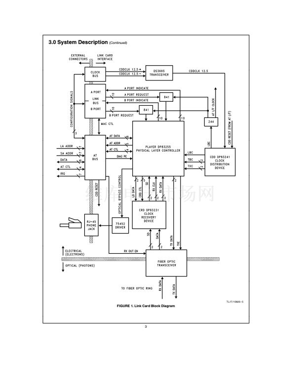
3 1 Block Diagram Description
3 2 At Interface Block
3 3 Clock Bus Block
3 4 CDD Device Block
3 5 CRD Device Block
3 6 Link Bus Block
3 7 PLAYER
TM
Device Block
3 8 Transceiver Block
4 0 APPENDICES
A Board Specifics
1 Installation
2 Layout Considerations
3 Pinouts
D Point to Point Applications
E Configuration Diagrams
F Board Schematics
1 Circuit Schematics
2 Layout Plots
G At Interface GAL Equations
H Component Inventory
PLAYER
TM
is a trademark of National Semiconductor Corporation
C
1995 National Semiconductor Corporation
TL F 10826
RRD-B30M105 Printed in U S A


 1
1
 2
2
 3
3
 4
4
 5
5
 6
6
