DMN100
N-CHANNEL ENHANCEMENT MODE FIELD EFFECT
TRANSISTOR
Features
路
路
路
Extremely Low On-Resistance:
170mW @ V
GS
= 4.5V
High Drain Current: 1.1A
Ideal for Notebook Computer, Portable Phone,
PCMCIA Cards, and Battery Powered Circuits
SC-59
A
D
TOP VIEW
B
S
D
G
H
K
J
L
M
C
Dim
A
B
C
D
E
G
H
J
K
L
M
Min
0.30
1.40
2.50
0.85
0.30
1.70
2.70
戮
1.00
0.55
0.10
Max
0.50
1.80
3.00
1.05
0.70
2.10
3.10
0.10
1.40
0.70
0.35
Mechanical Data
路
路
路
路
路
路
Case: SC-59, Molded Plastic
Case Material - UL Flammability Rating
Classification 94V-0
Terminals: Solderable per MIL-STD-202,
Method 208
Terminal Connections: See Diagrams
Weight: 0.008 grams (approx.)
Ordering Information, See Sheet 2
G
E
All Dimensions in mm
Maximum Ratings
Drain-Source Voltage
Gate-Source Voltage
Drain Current
Total Power Dissipation
@ T
A
= 25擄C unless otherwise specified
Symbol
V
DSS
Continuous
Continuous
Pulsed
V
GSS
I
D
P
d
R
qJA
T
j
, T
STG
DMN100
30
鹵20
鹵
1.1
鹵
4.0
500
250
-55 to +150
Units
V
V
A
mW
K/W
擄C
Characteristic
Thermal Resistance, Junction to Ambient
Operating and Storage Temperature Range
Notes:
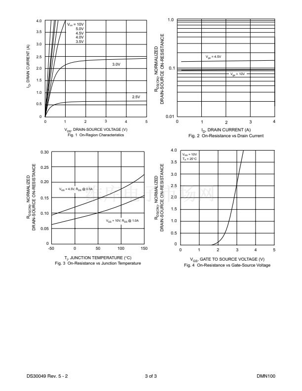
1. Pulse width
攏
300ms, duty cycle
攏
2%.
DS30049 Rev. 5 - 2
1 of 3
DMN100


 1
1
 2
2
 3
3
