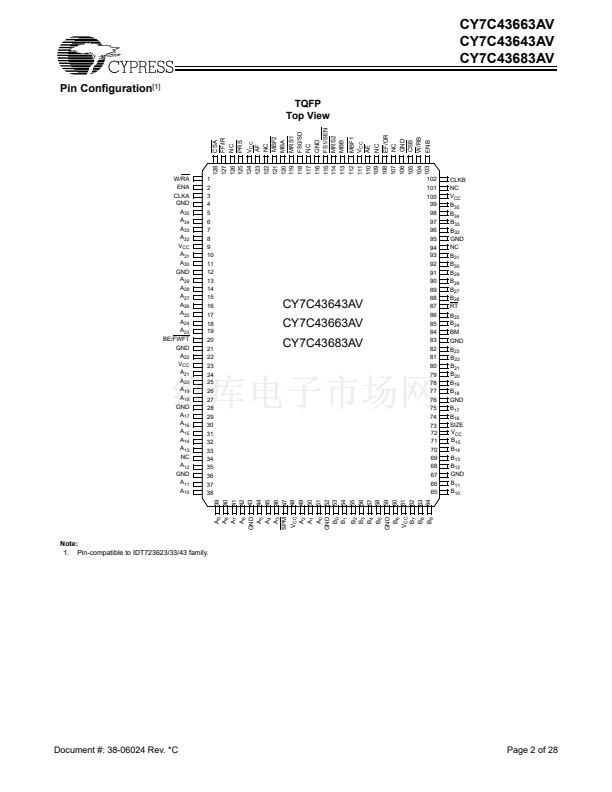
鈥?/div>
鈥?I
CC
= 60 mA
鈥?I
SB
= 10 mA
Fully asynchronous and simultaneous Read and Write
operation permitted
Mailbox bypass register for each FIFO
Parallel and serial programmable Almost Full and
Almost Empty flags
Retransmit function
Standard or FWFT user selectable mode
Partial reset
Big or Little Endian format for word or byte bus sizes
128-pin TQFP packaging
Easily expandable in width and depth
Logic Block Diagram
MBF1
CLKA
CSA
W/RA
ENA
MBA
RT
Input
Register
Output
Register
1K/4K/16K
脳 36
Dual Ported
Memory
Bus Matching
Port A
Control
Logic
Mail1
Register
CLKB
CSB
W/RB
ENB
MBB
BM
SIZE
Port B
Control
Logic
MRS1
MRS2
PRS
FIFO,
Mail1
Mail2
Reset
Logic
Write
Pointer
Read
Pointer
FF/IR
AF
Status
Flag Logic
36
Programmable
Flag Offset
Registers
Timing
Mode
EF/OR
AE
SPM
FS0/SD
FS1/SEN
A
0鈥?5
B
0鈥?5
BE/FWFT
36
Mail2
Register
MBF2
Cypress Semiconductor Corporation
Document #: 38-06024 Rev. *C
鈥?/div>
3901 North First Street
鈥?/div>
San Jose
鈥?/div>
CA 95134 鈥?408-943-2600
Revised December 26, 2002


 1
1
 2
2
 3
3
 4
4
 5
5
 6
6
 7
7
 8
8
 9
9
 10
10
 11
11
 12
12
 13
13
 14
14
 15
15
 16
16
 17
17
 18
18
 19
19
 20
20
 21
21
 22
22
 23
23
 24
24
 25
25
 26
26
 27
27
 28
28
