PRELIMINARY
CY7C1461V33
CY7C1463V33
CY7C1465V33
1M x 36/2M x 18/512K x 72 Flow-Thru SRAM
with NoBL鈩?Architecture
Features
鈥?Zero Bus Latency錚? no dead cycles between Write and
Read cycles
鈥upports 133-MHz bus operations
鈥?M 脳 36/2M 脳 18/512K 脳 72 common I/O
鈥ast clock-to-output times
鈥?6.5 ns (for 133-MHz device)
鈥?7.5 ns (for 117-MHz device)
鈥?Single 3.3V 鈥?% and +5% power supply V
DD
鈥?Separate V
DDQ
for 3.3V or 2.5V
鈥?Clock Enable (CEN) pin to suspend operation
鈥?Burst Capability鈥搇inear or interleaved burst order
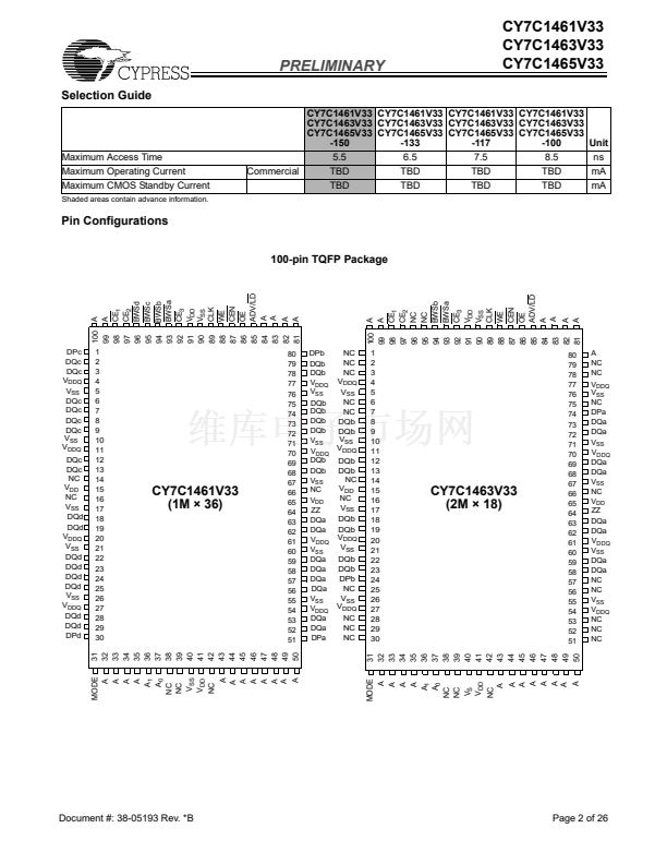
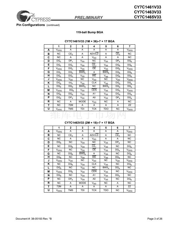
鈥?Available in 119-ball bump BGA, 165-ball FBGA, and
100-pin TQFP packages (CY7C1461V33 and
CY7C1463V33). 209-ball FBGA package for
CY7C1465V33.
BWS
c
,BWS
d,
BWS
e
, BWS
f
, BWS
g
, BWS
h
), and Read-Write
control (WE). BWS
c
and BWS
d
apply to CY7C1461V33 and
CY7C1465V33 only. BWS
e
, BWS
f,
BWS
g
and BWS
h
apply to
CY7C1465V33 only
A Clock Enable (CEN) pin allows operation of the
CY7C1461V33, CY7C1463V33, and CY7C1465V33 to be
suspended as long as necessary. All synchronous inputs are
ignored when (CEN) is high and the internal device registers
will hold their previous values.
There are three Chip Enable (CE
1
, CE
2
, CE
3
) pins that allow
the user to deselect the device when desired. If any one of
these three are not active when ADV/LD is low, no new
memory operation can be initiated and any burst cycle in
progress is stopped. However, any pending data transfers
(READ or WRITE) will be completed. The data bus will be in
high impedance state two cycles after chip is deselected or a
Write cycle is initiated.
The CY7C1461V33, CY7C1463V33 and CY7C1465V33 have
an on-chip two-bit burst counter. In the burst mode,
CY7C1461V33, CY7C1463V33 and CY7C1465V33 provide
four cycles of data for a single address presented to the
SRAM. The order of the burst sequence is defined by the
MODE input pin. The MODE pin selects between linear and
interleaved burst sequence. The ADV/LD signal is used to load
a new external address (ADV/LD = LOW) or increment the
internal burst counter (ADV/LD = HIGH)
Output Enable (OE) and burst sequence select (MODE) are
the asynchronous signals. OE can be used to disable the
outputs at any given time. ZZ may be tied to LOW if it is not
used.
Four pins are used to implement JTAG test capabilities. The
JTAG circuitry is used to serially shift data to and from the
device. JTAG inputs use LVTTL/LVCMOS levels to shift data
during this testing mode of operation.
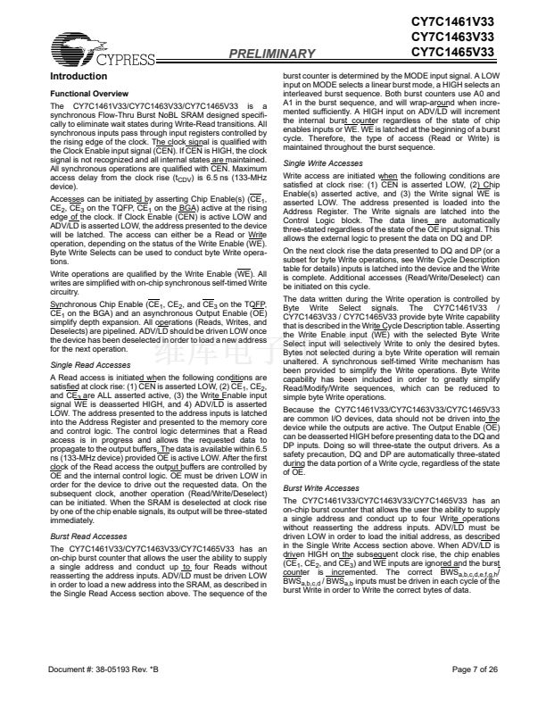
Functional Description
The CY7C1461V33, CY7C1463V33 and CY7C1465V33
SRAMs are designed to eliminate dead cycles when transi-
tions from Read to Write or vice versa. These SRAMs are
optimized for 100% bus utilization and achieve Zero Bus
Latency. They integrate 1,048,576 脳 36/2,097,152 脳 18/
524,288 脳 72 SRAM cells, respectively, with advanced
synchronous peripheral circuitry and a two-bit counter for
internal burst operation. The Synchronous Burst SRAM family
employs high-speed, low-power CMOS designs using
advanced single layer polysilicon, threelayer metal
technology. Each memory cell consists of six transistors.
All synchronous inputs are gated by registers controlled by a
positive-edge-triggered Clock Input (CLK). The synchronous
inputs include all addresses, all data inputs, depth-expansion
Chip Enables (CE
1
, CE
2
and CE
3
), cycle start input (ADV/LD),
Clock Enable (CEN), Byte Write Selects (BWS
a
, BWS
b
,
Logic Block Diagram
CLK
CE
ADV/LD
A
x
CEN
CE
1
CE2
BWS
X
CE3
WE
CONTROL
and WRITE
LOGIC
1M 脳 36
2M 脳 18
512K 脳 72
Memory
Array
D
Data-In REG.
Q
A
X
1M脳36
2M脳18
X = 19:0
DQ
X
DP
X
X = a, b, X= a, b, X = a, b
, c, d
c, d
c, d
BWS
x
Mode
DQ
x
DP
x
X = 20:0 X = a, b X = a, b X = a, b
X = a, b, X = a, b
512K脳72
X = 18:0 X = a, b,
c,d,e,f,g,h c,d,e,f,g,h c,d,e,f,g,h
OE
Cypress Semiconductor Corporation
Document #: 38-05193 Rev. *B
鈥?/div>
3901 North First Street
鈥?/div>
San Jose
鈥?/div>
CA 95134 鈥?408-943-2600
Revised November 18, 2002


 1
1
 2
2
 3
3
 4
4
 5
5
 6
6
 7
7
 8
8
 9
9
 10
10
 11
11
 12
12
 13
13
 14
14
 15
15
 16
16
 17
17
 18
18
 19
19
 20
20
 21
21
 22
22
 23
23
 24
24
 25
25
 26
26
