PRELIMINARY
CY7C1441V33
CY7C1443V33
CY7C1447V33
1M x 36/2M x 18/512K x 72
Flow-through SRAM
Features
鈥?Supports 133-MHz bus operations
鈥?1M x 36/2M x 18/512K x 72 common I/O
鈥?Fast clock-to-output times
鈥?6.5 ns (for 133-MHz device)
鈥?7.5 ns (for 117-MHz device)
鈥?Single 3.3V 鈥?% and +5% power supply V
DD
鈥?Separate V
DDQ
for 3.3V or 2.5V
鈥?Byte Write Enable and Global Write control
鈥?Burst Capability 鈥?linear or interleaved burst order
鈥?Automatic power down available using ZZ mode or CE
deselect
鈥?JTAG boundary scan for BGA packaging version
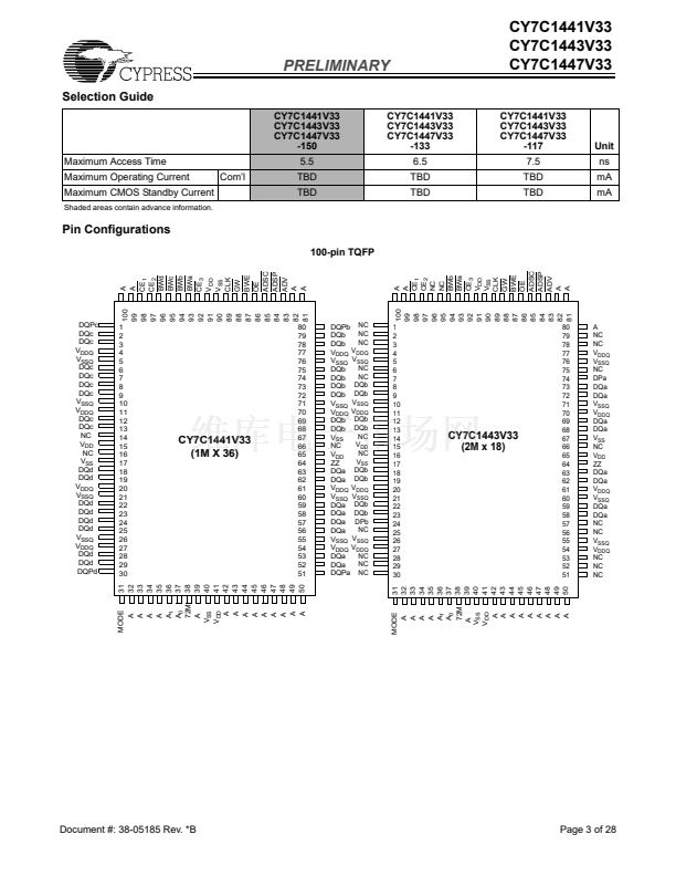
鈥?Available in 119-ball bump BGA, 165-ball FBGA, and
100-pin TQFP packages (CY7C1441V33 and
CY7C1443V33). 209 FBGA package for CY7C1447V33.
inputs include all addresses, all data inputs, address-pipelining
Chip Enable (CE), Burst Control Inputs (ADSC, ADSP, and
ADV), Write Enables (BW
a
, BW
b
, BW
c
, BW
d
, BW
e
, BW
f
, BW
g
,
BW
h
, and BWe), and Global Write (GW).
Asynchronous inputs include the Output Enable (OE) and
Burst Mode Control (MODE). The data outputs (DQ), enabled
by OE, are also asynchronous.
Addresses and chip enables are registered with either
Address Status Processor (ADSP) or address status controller
(ADSC) input pins. Subsequent burst addresses can be inter-
nally generated as controlled by the Burst Advance Pin (ADV).
Address, data inputs, and write controls are registered on-chip
to initiate self-timed Write cycle. Write cycles can be one to
four bytes wide as controlled by the write control inputs.
Individual byte write allows individual byte to be written. BW
a
controls DQ1鈥揇Q8 and DP1. BW
b
controls DQ9鈥揇Q16 and
DP2. BW
c
controls DQ17鈥揇Q24 and DP3. BW
d
controls
DQ25鈥揇Q32 and DP4. BW
e
controls DQ33鈥揇Q40 and DP5.
BW
f
controls DQ41鈥揇Q48 and DP6. BW
g
controls
DQ49鈥揇Q56 and DP7. BW
h
controls DQ57鈥揇Q64 and DP8.
BW
a
, BW
b
, BW
c
, BW
d
, BW
e
, BW
f
, BW
g
, and BW
h
can be
active only with BWE being LOW. GW being LOW causes all
bytes to be written. Write pass-through capability allows
written data available at the output for the immediately next
Read cycle. This device also incorporates pipelined enable
circuit for easy depth expansion without penalizing system
performance.
All inputs and outputs of theCY7C1441V33/CY7C1443V33/
CY7C1447V33 are JEDEC-standard JESD8-5-compatible.
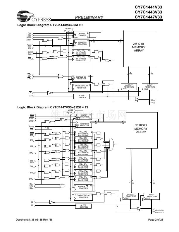
Functional Description
The Cypress Synchronous Burst SRAM family employs
high-speed, low power CMOS designs using advanced
single-layer polysilicon, triple-layer metal technology. Each
memory cell consists of six transistors.
The CY7C1441V33/CY7C1443V33/CY7C1447V33 SRAMs
integrate 1,048,576 x 36/2,097,152 x18 and 524,288 x 72
SRAM cells with advanced synchronous peripheral circuitry
and a two-bit counter for internal burst operation. All
synchronous inputs are gated by registers controlled by a
positive-edge-triggered clock input (CLK). The synchronous
Logic Block Diagram CY7C1441V33 鈥?1M 脳 36
MODE
(A
[1;0]
) 2
CLK
ADV
ADSC
ADSP
A
[19:0]
GW
BWE
BW
d
BW
c
D
BW
b
D
BW
a
CE
1
CE
2
CE
3
D
BURST Q
0
CE COUNTER
Q
1
CLR
Q
20
18
D
ADDRESS
CE REGISTER
D
DQ
d
, DP
d
BYTEWRITE
REGISTERS
DQ
c
, DP
c
BYTEWRITE
REGISTERS
DQ
b
, DP
b
BYTEWRITE
REGISTERS
DQ
a
, DP
a
BYTEWRITE
REGISTERS
ENABLE CE
REGISTER
Q
18
20
1M X36
MEMORY
ARRAY
D
Q
Q
Q
36
Q
36
D ENABLE DELAY Q
REGISTER
OE
ZZ
SLEEP
CONTROL
OUTPUT
REGISTERS
CLK
INPUT
REGISTERS
CLK
DQ
a,b,c,d
DP
a,b,c,d
Cypress Semiconductor Corporation
Document #: 38-05185 Rev. *B
鈥?/div>
3901 North First Street
鈥?/div>
San Jose
,
CA 95134
鈥?/div>
408-943-2600
Revised November 13, 2002


 1
1
 2
2
 3
3
 4
4
 5
5
 6
6
 7
7
 8
8
 9
9
 10
10
 11
11
 12
12
 13
13
 14
14
 15
15
 16
16
 17
17
 18
18
 19
19
 20
20
 21
21
 22
22
 23
23
 24
24
 25
25
 26
26
 27
27
 28
28
