鈥?/div>
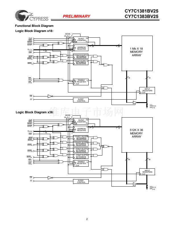
burst operation. All synchronous inputs are gated by registers
controlled by a positive-edge-triggered Clock Input (CLK). The
synchronous inputs include all addresses, all data inputs, ad-
dress-pipelining Chip Enable (CE), Burst Control Inputs (AD-
SC, ADSP and ADV), Write Enables (BWa, BWb, BWc,
,
BWd,and BWe), and Global Write (GW).
... Asynchronous inputs include the Output Enable (OE) and
burst Mode Control (MODE). The Data Outputs (Q), enabled
by OE, are also asynchronous.
Addresses and chip enables are registered with either Ad-
dress Status Processor (ADSP) or Address Status Controller
(ADSC) input pins. Subsequent burst addresses can be inter-
nally generated as controlled by the Burst Advance Pin (ADV).
Address, data inputs, and write controls are registered on-chip
to initiate self-timed WRITE cycle. WRITE cycles can be one
to four bytes wide as controlled by the write control inputs.
Individual byte write allows individual byte to be written. BWa
controls DQ1鈥揇Q8 and DQP1. BWb controls DQ9鈥揇Q16 and
DQP2. BWc controls DQ17鈥揇Q24and DQP3. BWd controls
DQ25鈥揇Q32 and DQP4. BWa, BWb BWc, and BWd can be
active only with BWe being LOW. GW being LOW causes all
bytes to be written. WRITE pass-through capability allows writ-
ten data available at the output for the immediately next READ
cycle. This device also incorporates pipelined enable circuit for
easy depth expansion without penalizing system performance.
All inputs and outputs of the CY7C1381BV25 and the
CY7C1383BV25 are JEDEC standard JESD8-5 compatible.
Functional Description
The Cypress Synchronous Burst SRAM family employs
high-speed, low power CMOS designs using advanced single
layer polysilicon, three-layer metal technology. Each memory
cell consists of six transistors.
The CY7C1381BV25 and CY7C1383BV25 SRAMs integrate
524,288x36 and 1,048,576x18SRAM cells with advanced syn-
chronous peripheral circuitry and a 2-bit counter for internal
Selection Guide
133 MHz
Maximum Access Time (ns)
Maximum Operating Current (mA)
Maximum CMOS Standby Current (mA)
Shaded areas contain advance information.
117 MHz
7.5
175
30
100 MHz
8.5
150
30
6.5
Commercial
200
30
Cypress Semiconductor Corporation
鈥?/div>
3901 North First Street
鈥?/div>
San Jose
鈥?/div>
CA 95134
鈥?/div>
408-943-2600
July 2, 2001


 1
1
 2
2
 3
3
 4
4
 5
5
 6
6
 7
7
 8
8
 9
9
 10
10
 11
11
 12
12
 13
13
 14
14
 15
15
 16
16
 17
17
 18
18
 19
19
 20
20
 21
21
 22
22
 23
23
 24
24
 25
25
 26
26
 27
27
 28
28
