鈥?/div>
鈥?8.5 ns (for 100-MHz device)
Clock Enable (CEN) pin to suspend operation
Synchronous self-timed writes
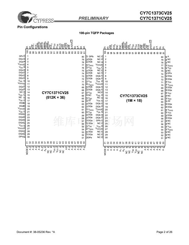
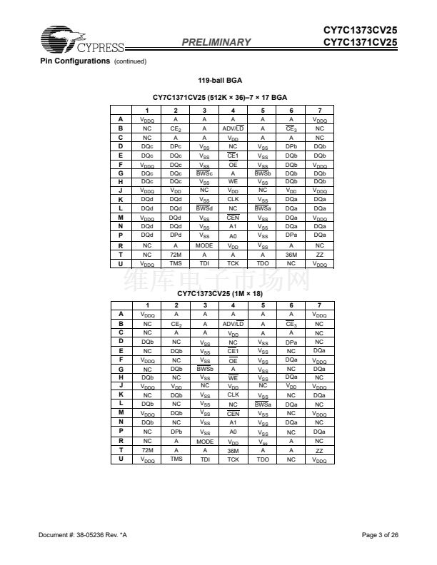
Available in 100 TQFP and 119 BGA Packages
Burst Capability 鈥?linear or interleaved burst order
JTAG boundary scan for BGA packaging version
respectively designed specifically to support unlimited true
back-to-back Read/Write operations without the insertion of
wait states. The CY7C1371CV25/CY7C1373CV25 is
equipped with the advanced No Bus Latency鈩?(NoBL鈩? logic
required to enable consecutive Read/Write operations with
data being transferred on every clock cycle. This feature
dramatically improves the throughput of data through the
SRAM, especially in systems that require frequent Write/Read
transitions.
The
CY7C1371CV25/CY7C1373CV25
is
pin-compatible and functionally equivalent to ZBT devices.
All synchronous inputs pass through input registers controlled
by the rising edge of the clock.The clock input is qualified by
the Clock Enable (CEN) signal, which when deasserted
suspends operation and extends the previous clock cycle.
Maximum access delay from the clock rise is 6.5 ns (133-MHz
device).
Write operations are controlled by the Byte Write Selects
for
CY7C1371CV25
and
BWS
a,b
for
(BWS
a,b,c,d
CY7C1373CV25) and a Write Enable (WE) input. All writes are
conducted with on-chip synchronous self-timed write circuitry.
ZZ may be tied to LOW if it is not used.
Synchronous Chip Enable (CE
1
, CE
2
, CE
3
on the TQFP, CE
1
on the BGA) and an asynchronous Output Enable (OE)
provide for easy bank selection and output three-state control.
In order to avoid bus contention, the output drivers are
synchronously three-stated during the data portion of a write
sequence.
Functional Description
The CY7C1371CV25 and CY7C1373CV25 are 2.5V, 512K by
36 and 1M by 18 Synchronous-Flow-Through Burst SRAMs,
Logic Block Diagram
CLK
CE
ADV/LD
A
x
CEN
CE
1
CE2
CE3
WE
BWS
x
Mode
CONTROL
and WRITE
LOGIC
256K 脳 36/
512K 脳 18
MEMORY
ARRAY
D
Data-In REG.
Q
AX
DQX
CY7C1371
X = 18:0
CY7C1373
X = 19:0
DQ
x
DP
x
X= a, b, c, d X = a, b
DPX X = a, b, c, d X = a, b
BWSX X = a, b, c, d X = a, b
OE
Selection Guide
133 MHz
Maximum Access Time
Maximum Operating Current
Maximum CMOS Standby Current
Shaded areas contain preliminary information.
117 MHz
7.5
190
70
100 MHz
8.5
175
70
Unit
ns
mA
mA
6.5
210
70
.
Cypress Semiconductor Corporation
Document #: 38-05236 Rev. *A
鈥?/div>
3901 North First Street
鈥?/div>
San Jose, CA 95134
鈥?/div>
408-943-2600
Revised November 20, 2002


 1
1
 2
2
 3
3
 4
4
 5
5
 6
6
 7
7
 8
8
 9
9
 10
10
 11
11
 12
12
 13
13
 14
14
 15
15
 16
16
 17
17
 18
18
 19
19
 20
20
 21
21
 22
22
 23
23
 24
24
 25
25
 26
26
