錚?/div>
interleaved or linear burst sequences
鈥?Multiple chip enables for depth expansion: three chip
enables for A package version and two chip enables for
AJ package version
鈥?Separate processor and controller address strobes
鈥?Synchronous self-timed writes
鈥?Asynchronous Output Enable
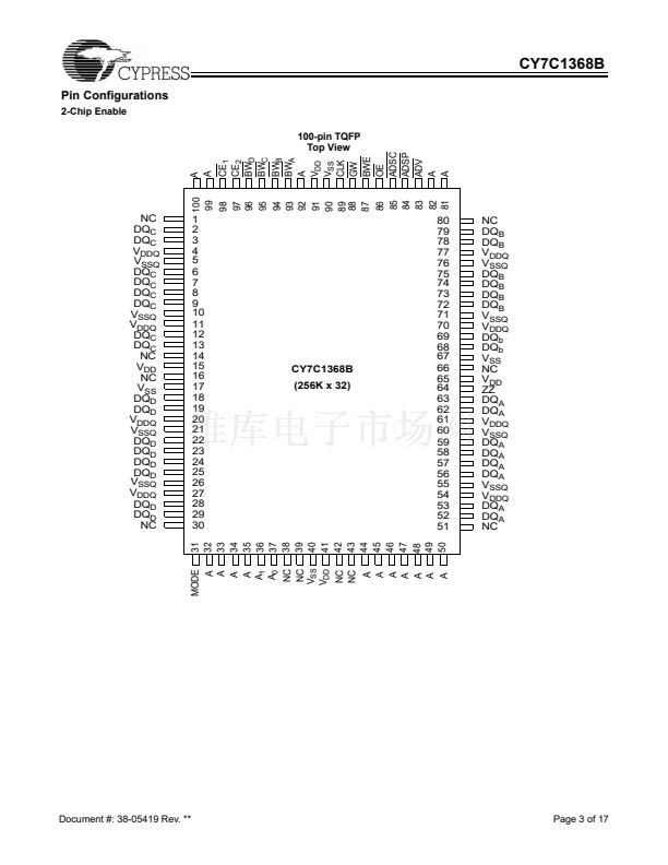
鈥?JEDEC-standard 100-pin TQFP package and pinout
鈥?鈥淶Z鈥?Sleep Mode option
Functional Description
[1]
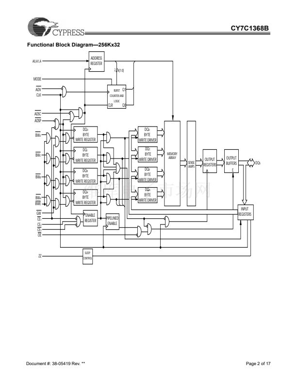
The CY7C1368B SRAM integrates 262,144 x 32 SRAM cells
with advanced synchronous peripheral circuitry and a two-bit
counter for internal burst operation. All synchronous inputs are
gated by registers controlled by a positive-edge-triggered
Clock Input (CLK). The synchronous inputs include all
addresses, all data inputs, address-pipelining Chip Enable
(CE
1
), depth-expansion Chip Enables (CE
2
and CE
3 [2]
), Burst
Control inputs (ADSC, ADSP, and ADV), Write Enables (BW
A
,
BW
B
, BW
C
, BW
D
and BWE), and Global Write (GW).
Asynchronous inputs include the Output Enable (OE) and the
ZZ pin.
Addresses and chip enables are registered at rising edge of
clock when either Address Strobe Processor (ADSP) or
Address Strobe Controller (ADSC) are active. Subsequent
burst addresses can be internally generated as controlled by
the Advance pin (ADV).
Address, data inputs, and write controls are registered on-chip
to initiate a self-timed Write cycle. This part supports Byte
Write operations (see Pin Descriptions and Truth Table for
further details). Write cycles can be one to four bytes wide as
controlled by the byte write control inputs. GW active LOW
causes all bytes to be written. This device incorporates an
additional pipelined enable register which delays turning off
the output buffers an additional cycle when a deselect is
executed.This feature allows depth expansion without penal-
izing system performance.
The CY7C1368B operates from a +3.3V core power supply
and a +3.3V supply for the I/Os. All inputs and outputs are
JEDEC-standard JESD8-5-compatible.
Selection Guide
200 MHz
Maximum Access Time
Maximum Operating Current
Maximum CMOS Standby Current
3.0
220
30
166 MHz
3.5
180
30
Unit
ns
mA
mA
Notes:
1. For best-practice recommendations, please refer to the Cypress application note 鈥淪ystem Design Guidelines鈥?on http://www.cypress.com.
2. CE
3
is for A version (3 Chip enable option) only
Cypress Semiconductor Corporation
Document #: 38-05419 Rev. **
鈥?/div>
3901 North First Street
鈥?/div>
San Jose
,
CA 95134
鈥?/div>
408-943-2600
Revised December 23, 2003


 1
1
 2
2
 3
3
 4
4
 5
5
 6
6
 7
7
 8
8
 9
9
 10
10
 11
11
 12
12
 13
13
 14
14
 15
15
 16
16
 17
17
