鈥?/div>
鈥?8.5 ns (for 100-MHz device)
Two-bit wrap-around counter supporting either inter-
leaved or linear burst sequences
Separate processor and controller address strobes
provide direct interface with the processor and external
cache controller
Synchronous self-timed writes
Asynchronous output enable
Single 3.3V power supply
Supports 3.3V or 2.5V I/Os
JEDEC-standard pinout
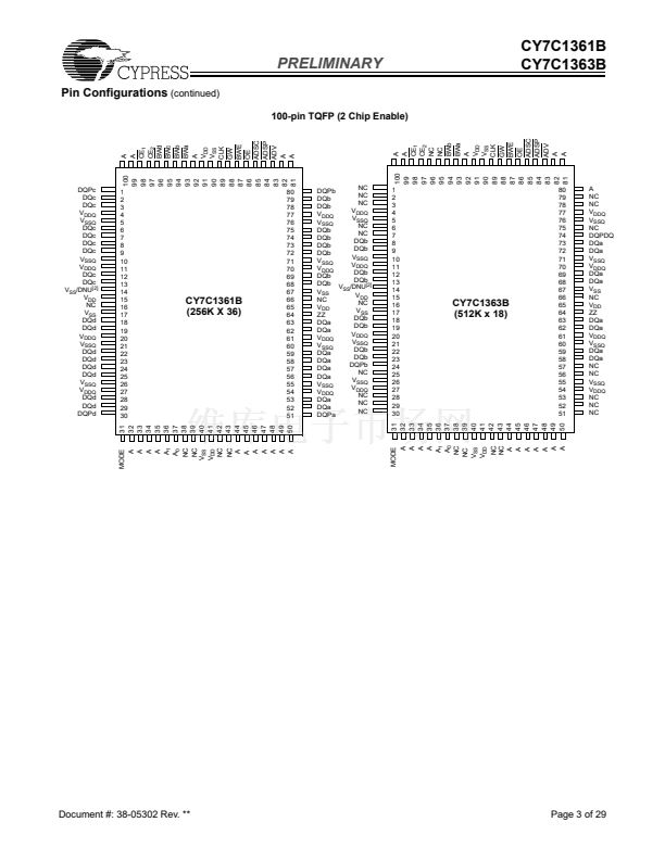
Available as a 100-pin TQFP, 119-ball BGA, and 165-ball
fBGA
鈥?Both 2 and 3 Chip Enable Options for TQFP
[1]
IEEE 1149.1 JTAG-compatible Boundary Scan
鈥?119-ball BGA and 165-ball fBGA
Functional Description
The CY7C1361B and CY7C1363B are 3.3V, 256K x 36 and
512K x 18 Synchronous Flowthrough SRAMs, respectively,
designed to interface with high-speed microprocessors with
minimal glue logic. Maximum access delay from the clock rise
is 6.5 ns (133-MHz device). A two-bit on-chip wraparound
burst counter captures the first address in a burst sequence
and automatically increments the address for the rest of the
burst access.
The CY7C1361B/CY7C1363B supports either the interleaved
or linear burst sequences, selected by the MODE input pin. A
HIGH selects an interleaved burst sequence, while a LOW
selects a linear burst sequence. Burst accesses can be
initiated by asserting either the Processor Address Strobe
(ADSP) or the Controller Address Strobe (ADSC) at clock rise.
Address advancement through the burst sequence is
controlled by the ADV input. Byte write operations are qualified
with the Byte Write Select (BW
a,b,c,d
for CY7C1361B and
BW
a,b
for CY7C1363B) inputs. A Global Write Enable (GW)
overrides all byte write inputs and writes data to all four bytes.
All writes are conducted with on-chip synchronous self-timed
write circuitry.
Three synchronous Chip Selects (CE
1
, CE
2
, CE
3[1]
) and an
asynchronous output enable (OE) provide for easy bank
selection and output three-state control.
鈥?/div>
Logic Block Diagram
CLK
ADV
A
x
GW
CE
1
CE
2
CE
3
BWE
7C1363B
BW
x
A
[18:0]
MODE
ADSP
DQ
a,b
ADSC
DQP
a,b
ZZ
BW
a,b
OE
CONTROL
and WRITE
LOGIC
D
CE
Data-In REG.
Q
256Kx36/
512Kx18
MEMORY
ARRAY
DQ
x
DQP
x
A
X
DQ
X
DQP
X
BW
X
7C1361B
A
[17:0]
DQ
a,b,c,d
DQP
a,b,c,d
BW
a,b,c,d
Selection Guide
7C1361B-133
7C1363B-133
Maximum Access Time
Maximum Operating Current
Maximum CMOS Standby Current
Note:
1. CE3 not available on 2 Chip Enable TQFP package or 119 BGA.
7C1361B-117
7C1363B-117
7.5
220
30
7C1361B-100
7C1363B-100
8.5
180
30
Unit
ns
mA
mA
6.5
Commercial
250
30
Cypress Semiconductor Corporation
Document #: 38-05302 Rev. **
鈥?/div>
3901 North First Street
鈥?/div>
San Jose
鈥?/div>
CA 95134 鈥?408-943-2600
Revised August 16, 2002


 1
1
 2
2
 3
3
 4
4
 5
5
 6
6
 7
7
 8
8
 9
9
 10
10
 11
11
 12
12
 13
13
 14
14
 15
15
 16
16
 17
17
 18
18
 19
19
 20
20
 21
21
 22
22
 23
23
 24
24
 25
25
 26
26
 27
27
 28
28
 29
29
