鈥?/div>
鈥?5.0 ns (for 100-MHz device)
Clock Enable (CEN) pin to suspend operation
Synchronous self-timed writes
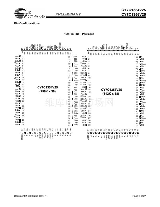
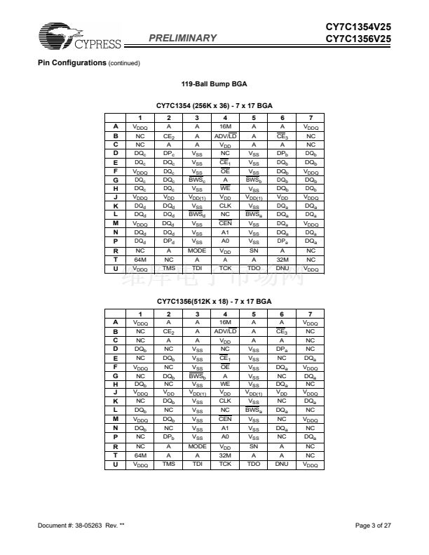
Available in 100 TQFP & 119 BGA Packages
Burst Capability鈥攍inear or interleaved burst order
spectively. They are designed specifically to support unlimited
true back-to-back Read/Write operations without the insertion
of wait states. The CY7C1354V25/CY7C1356V25 is equipped
with the advanced No Bus Latency鈩?(NoBL鈩? logic required
to enable consecutive Read/Write operations with data being
transferred on every clock cycle. This feature dramatically im-
proves the throughput of data through the SRAM, especially in
systems that require frequent Write/Read transitions. The
CY7C1354V25/CY7C1356V25 is pin compatible and function-
ally equivalent to ZBT devices.
All synchronous inputs pass through input registers controlled
by the rising edge of the clock. All data outputs pass through
output registers controlled by the rising edge of the clock. The
clock input is qualified by the Clock Enable (CEN) signal, which
when deasserted suspends operation and extends the previ-
ous clock cycle. Maximum access delay from the clock rise is
3.2 ns (200-MHz device).
Write operations are controlled by the Byte Write Selects
(BWS
a
鈥揃WS
d
for CY7C1354V25 and BWS
a
鈥揃WS
b
for
CY7C1356V25) and a Write Enable (WE) input. All writes are
conducted with on-chip synchronous self-timed write circuitry.
Three synchronous Chip Enables (CE
1
, CE
2
, CE
3
) and an
asynchronous Output Enable (OE) provide for easy bank se-
lection and output three-state control. In order to avoid bus
contention, the output drivers are synchronously three-stated
during the data portion of a write sequence.
Functional Description
The CY7C1354V25 and CY7C1356V25 are 2.5V, 256K by 36
and 512K by 18 Synchronous-Pipelined Burst SRAMs, re-
Logic Block Diagram
CLK
CE
ADV/LD
A
x
CEN
CE
1
CE
2
CE
3
WE
BWS
x
Mode
CONTROL
and WRITE
LOGIC
256KX36/
512KX18
MEMORY
ARRAY
OUTOUT
REGISTERS
and LOGIC
D
Data-In REG.
Q
DQ
x
DP
x
CY7C1354
A
X
DQ
X
DP
X
BWS
X
X = 17:0
X = a, b, c, d
X = a, b, c, d
X = a, b, c, d
CY7C1356
X = 18:0
X = a, b
X = a, b
X = a, b
OE
.
Selection Guide
7C1354V25-200 7C1354V25-166 7C1354V25-133 7C1354V25-100
7C1356V25-200 7C1356V25-166 7C1356V25-133 7C1356V25-100
Maximum Access Time (ns)
Maximum Operating Current (mA)
Com鈥檒
Maximum CMOS Standby Current (mA) Com鈥檒
3.2
475
10
3.5
450
10
4.0
370
10
5.0
300
10
Shaded areas contain advance information.
No Bus Latency and NoBL are trademarks of Cypress Semiconductor Corporation.
ZBT is a trademark of Integrated Device Technology.
Cypress Semiconductor Corporation
Document #: 38-05263 Rev. **
鈥?/div>
3901 North First Street
鈥?/div>
San Jose
鈥?/div>
CA 95134 鈥?408-943-2600
Revised March 6, 2002


 1
1
 2
2
 3
3
 4
4
 5
5
 6
6
 7
7
 8
8
 9
9
 10
10
 11
11
 12
12
 13
13
 14
14
 15
15
 16
16
 17
17
 18
18
 19
19
 20
20
 21
21
 22
22
 23
23
 24
24
 25
25
 26
26
 27
27
