鈥?/div>
7.5 ns (for 117- MHz device)
鈥?8.5 ns (for 100-MHz device)
鈥?11.0 ns (for 66-MHz device)
鈥?12. 0 ns (for 50-MHz device)
鈥?14.0 ns (for 40-MHz device)
鈥?Clock Enable (CEN) pin to suspend operation
鈥?Synchronous self-timed writes
鈥?Asynchronous Output Enable
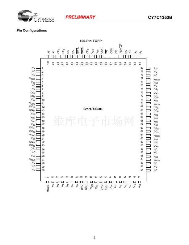
鈥?JEDEC-standard 100 TQFP package
鈥?Burst Capability鈥攍inear or interleaved burst order
鈥?Low standby power
Functional Description
The CY7C1353B is a 3.3V, 256K by 18 Synchronous
Flow-Through Burst SRAM designed specifically to support
unlimited true back-to-back Read/Write operations without the
insertion of wait states. The CY7C1353B is equipped with the
advanced No Bus Latency鈩?(NoBL鈩? logic required to en-
able consecutive Read/Write operations with data being trans-
ferred on every clock cycle. This feature dramatically improves
the throughput of data through the SRAM, especially in sys-
tems that require frequent Write-Read transitions. The
CY7C1353B is pin/functionally compatible to ZBT SRAMs
MCM63Z819 and MT55L256L18F.
All synchronous inputs pass through input registers controlled
by the rising edge of the clock. The clock input is qualified by
the Clock Enable (CEN) signal, which when deasserted sus-
pends operation and extends the previous clock cycle. Maxi-
mum access delay from the clock rise is 7.5 ns (117-MHz de-
vice).
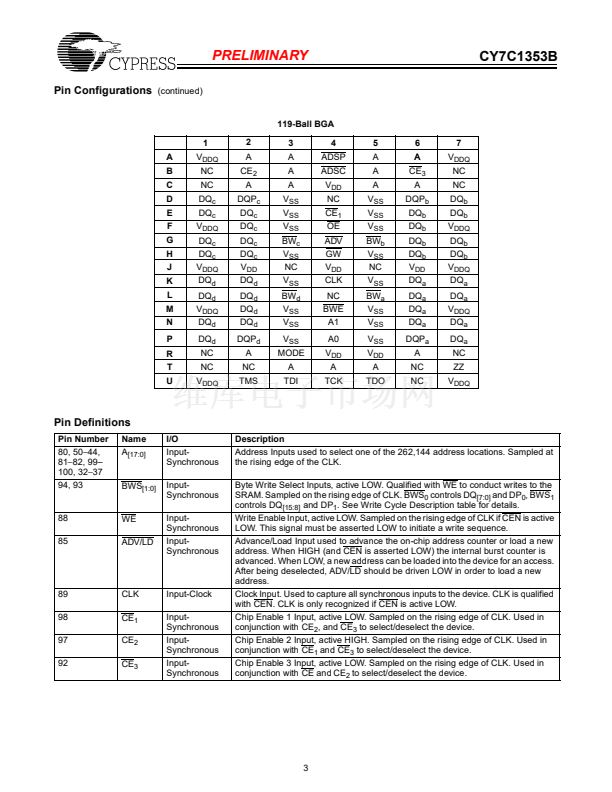
Write operations are controlled by the four Byte Write Select
(BWS
[1:0]
) and a Write Enable (WE) input. All writes are con-
ducted with on-chip synchronous self-timed write circuitry.
Three synchronous Chip Enables (CE
1
, CE
2
, CE
3
) and an
asynchronous Output Enable (OE) provide for easy bank se-
lection and output three-state control. In order to avoid bus
contention, the output drivers are synchronously three-stated
during the data portion of a write sequence.
Logic Block Diagram
CLK
D
Data-In REG.
CE Q
18
18
CONTROL
and WRITE
LOGIC
256KX18
MEMORY
ARRAY
18
DQ
[15:0]
DP
[1:0]
18
ADV/LD
A
[17:0]
CEN
CE1
CE 2
CE 3
WE
BWS [1:0]
Mode
18
OE
Selection Guide
7C1353B-117
Maximum Access Time (ns)
Maximum Operating Current (mA) Commercial
Maximum CMOS Standby
Current (mA)
Commercial
7.5
375
5
7C1353B-100
8.5
350
5
7C1353B-66 7C1353B-50 7C1353B-40
11.0
250
5
12.0
200
5
14.0
175
5
NoBL and No Bus Latency are trademarks of Cypress Semiconductor Corporation.
ZBT is a trademark of Integrated Device Technology.
Cypress Semiconductor Corporation
鈥?/div>
3901 North First Street
鈥?/div>
San Jose
鈥?/div>
CA 95134
鈥?/div>
408-943-2600
April 4, 2000


 1
1
 2
2
 3
3
 4
4
 5
5
 6
6
 7
7
 8
8
 9
9
 10
10
 11
11
 12
12
 13
13
 14
14
