鈥?/div>
Fast access times: 3.5, 3.8, and 4.0 ns
Fast clock speed: 166, 150, 133, and 117 MHz
Provide high performance 3-1-1-1 access rate
Fast OE access times: 3.5 ns and 3.8 ns
Optimal for performance (double cycle chip deselect,
depth expansion without wait state)
3.3V 鈥?% and +10% core power supply
2.5V or 3.3V I/O supply
5V tolerant inputs except I/Os
Clamp diodes to V
SSQ
at all inputs and outputs
Common data inputs and data outputs
Byte Write Enable and Global Write control
Three chip enables for depth expansion and address
pipeline
Address, data and control registers
Internally self-timed Write Cycle
Burst control pins (interleaved or linear burst se-
quence)
Automatic power-down for portable applications
High-density, high-speed packages
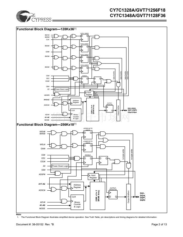
and a 2-bit counter for internal burst operation. All synchro-
nous inputs are gated by registers controlled by a posi-
tive-edge-triggered Clock Input (CLK). The synchronous in-
puts include all addresses, all data inputs, address-pipelining
Chip Enable (CE), depth-expansion Chip Enables (CE2 and
CE2), Burst Control inputs (ADSC, ADSP, and ADV), Write En-
ables (BW1, BW2, BW3, BW4, and BWE), and Global Write
(GW).
Asynchronous inputs include the Output Enable (OE) and
Burst Mode Control (MODE). The data outputs (Q), enabled
by OE, are also asynchronous.
Addresses and chip enables are registered with either Ad-
dress Status Processor (ADSP) or Address Status Controller
(ADSC) input pins. Subsequent burst addresses can be inter-
nally generated as controlled by the Burst Advance pin (ADV).
Address, data inputs, and write controls are registered on-chip
to initiate self-timed WRITE cycle. WRITE cycles can be one
to four bytes wide as controlled by the write control inputs.
Individual byte write allows individual byte to be written. BW1
controls DQ1鈥揇Q8 and DQP1. BW2 controls DQ9鈥揇Q16 and
DQP2. BW3 controls DQ17鈥揇Q24 and DQP3. BW4 controls
DQ25鈥揇Q32 and DQP4. BW1, BW2, BW3, and BW4 can be
active only with BWE being LOW. GW being LOW causes all
bytes to be written. WRITE pass-through capability allows writ-
ten data available at the output for the immediately next READ
cycle. This device also incorporates pipelined enable circuit for
easy depth expansion without penalizing system performance.
The CY7C1348A/GVT71128F36/CY7C1328A/GVT71256F18
operates from a +3.3V core power supply and all outputs op-
erate on a +2.5V supply. All inputs and outputs are JEDEC
standard JESD8-5 compatible. The device is ideally suited for
486, Pentium廬, 680x0, and PowerPC鈩?systems and for sys-
tems that benefit from a wide synchronous data bus.
Functional Description
The Cypress Synchronous Burst SRAM family employs
high-speed, low-power CMOS designs using advanced tri-
ple-layer polysilicon, double-layer metal technology. Each
memory cell consists of four transistors and two high-valued
resistors.
The
CY7C1348A/GVT71128F36
and
CY7C1328A/
GVT71256F18 SRAM integrate 262,144x18 and 131,072x36
SRAM cells with advanced synchronous peripheral circuitry
Selection Guide
7C1328A-166
71256F18-3
7C1348A-166
71128F36-3
Maximum Access Time (ns)
Maximum Operating Current (mA)
Maximum CMOS Standby Current (mA)
Pentium is a registered trademark of Intel Corporation.
PowerPC is a trademark of International Business Machines, Incorporated.
7C1328A-150
71256F18-4
7C1348A-150
71128F36-4
3.8
400
10
7C1328A-133
71256F18-5
7C1348A-133
71128F36-5
4.0
375
10
7C1328A-117
71256F18-6
7C1348A-117
71128F36-6
4.0
350
10
3.5
425
10
Cypress Semiconductor Corporation
Document #: 38-05152 Rev. *B
鈥?/div>
3901 North First Street
鈥?/div>
San Jose
鈥?/div>
CA 95134 鈥?408-943-2600
Revised January 19, 2003


 1
1
 2
2
 3
3
 4
4
 5
5
 6
6
 7
7
 8
8
 9
9
 10
10
 11
11
 12
12
 13
13
