User-selectable burst counter supporting Intel錚?/div>
Pentium interleaved or linear burst sequences
Separate processor and controller address strobes
Synchronous self-timed writes
Asynchronous Output Enable
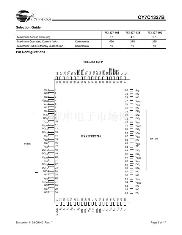
JEDEC-standard 100 TQFP pinout
鈥淶Z鈥?Sleep Mode option and Stop Clock option
The CY7C1327B I/O pins can operate at either the 2.5V or the
3.3V level. The I/O pins are 3.3V tolerant when V
DDQ
=2.5V.
All synchronous inputs pass through input registers controlled
by the rising edge of the clock. All data outputs pass through
output registers controlled by the rising edge of the clock. Max-
imum access delay from the clock rise is 3.5 ns (166-MHz
device).
The CY7C1327B supports either the interleaved burst se-
quence used by the Intel Pentium processor or a linear burst
sequence used by processors such as the PowerPC. The
burst sequence is selected through the MODE pin. Accesses
can be initiated by asserting either the Processor Address
Strobe (ADSP) or the Controller Address Strobe (ADSC) at
clock rise. Address advancement through the burst sequence
is controlled by the ADV input. A 2-bit on-chip wraparound
burst counter captures the first address in a burst sequence
and automatically increments the address for the rest of the
burst access.
Byte write operations are qualified with the four Byte Write
Select (BW
[1:0]
) inputs. A Global Write Enable (GW) overrides
all byte write inputs and writes data to all four bytes. All writes
are conducted with on-chip synchronous self-timed write cir-
cuitry.
Three synchronous Chip Selects (CE
1
, CE
2
, CE
3
) and an
asynchronous Output Enable (OE) provide for easy bank se-
lection and output three-state control. In order to provide prop-
er data during depth expansion, OE is masked during the first
clock of a read cycle when emerging from a deselected state.
Functional Description
The CY7C1327B is a 3.3V, 256K by 18 synchronous-pipelined
cache SRAM designed to support zero wait state secondary
cache with minimal glue logic.
Logic Block Diagram
CLK
ADV
ADSC
ADSP
A
[17:0]
GW
BWE
BW
1
BW
0
MODE
(A
[1;0]
) 2
BURST Q
0
CE COUNTER
Q
1
CLR
Q
ADDRESS
CE REGISTER
D
16
18
18
16
D DQ[15:8], DP[1] Q
BYTEWRITE
REGISTERS
D DQ[7:0], DP[0] Q
BYTEWRITE
REGISTERS
256KX18
MEMORY
ARRAY
CE
1
CE
2
CE
3
18
D
ENABLE CE
CE REGISTER
Q
18
D ENABLE DELAY Q
REGISTER
OE
ZZ
SLEEP
CONTROL
OUTPUT
REGISTERS
CLK
INPUT
REGISTERS
CLK
DQ
[15:0]
DP
[1:0]
Intel and Pentium are registered trademarks of Intel Corporation.
PowerPC is a trademark of IBM Corporation.
Cypress Semiconductor Corporation
Document #: 38-05140 Rev. **
鈥?/div>
3901 North First Street
鈥?/div>
San Jose
鈥?/div>
CA 95134 鈥?408-943-2600
Revised September 6, 2001


 1
1
 2
2
 3
3
 4
4
 5
5
 6
6
 7
7
 8
8
 9
9
 10
10
 11
11
 12
12
 13
13
 14
14
 15
15
 16
16
 17
17
