397V25
ADVANCE INFORMATION
CY7C1397V25
CY7C1322V25
18-Mb 2-Word Burst SRAM with DDR-I Architecture
Features
鈥?18-Mb Density (1M x 18, 512K x 36)
鈥?Supports concurrent transactions
鈥?300-MHz Clock for High Bandwidth
鈥?2-Word Burst for reducing address bus frequency
鈥?Double Data Rate (DDR) interfaces (data transferred at
600 MHz) @300 MHz
鈥?Two input clocks (K and K) for precise DDR timing
鈥?SRAM uses rising edges only
鈥?Two output clocks (C and C) accounts for clock skew
and flight time mismatches
鈥?Separate Port Selects for depth expansion
鈥?Synchronous internally self-timed writes
鈥?2.5V core power supply with HSTL Inputs and Outputs
鈥?Variable drive HSTL output buffers
鈥?Expanded HSTL output voltage (1.4V鈥揤
DD
)
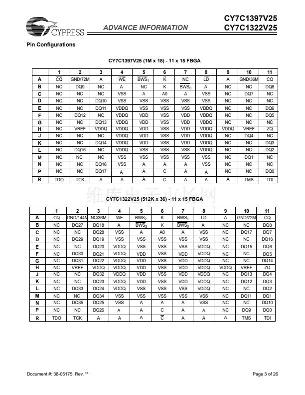
鈥?13x15 mm 1.0-mm pitch fBGA package, 165 ball (11x15
matrix)
鈥?JTAG Interface
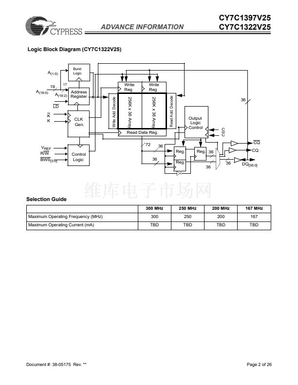
Functional Description
The CY7C1397V25/CY7C1322V25 are 2.5V Synchronous
Pipelined SRAMs equipped with DDR-I (Double Data Rate)
architecture. The DDR-I consists of an SRAM core with ad-
vanced synchronous peripheral circuitry and a 1-bit burst
counter. Addresses for Read and Write are latched on alter-
nate rising edges of the input (K) clock. Write data is registered
on the rising edges of both K and K. Read data is driven on the
rising edges of C and C if provided, or on the rising edge of K
and K if C/C are not provided. Every read or write operation is
associated with two words that burst sequentially into or out of
the device. The burst counter takes in the least significant bit
of the external address and bursts two 18-bit words in the case
of CY7C1397V25 and two 36-bit words in the case of
CY7C1322V25. Depth expansion is accomplished with Port
Selects for each port. Port selects allow each port to operate
independently.
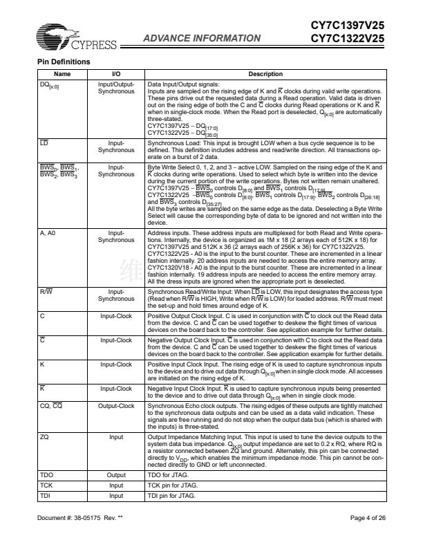
Asynchronous inputs include impedance match (ZQ). Syn-
chronous data outputs (Q, sharing the same physical pins as
the data inputs D) are tightly matched to the two output echo
clocks CQ/CQ, eliminating the need for separately capturing
data from each individual DDR SRAM in the system design.
Output data clocks (C/C) are also provided for maximum sys-
tem clocking and data synchronization flexibility.
All synchronous inputs pass through input registers controlled
by the K or K input clocks. All data outputs pass through output
registers controlled by the C or C input clocks. Writes are con-
ducted with on-chip synchronous self-timed write circuitry.
Configurations
CY7C1397V25 鈥?1M x 18
CY7C1322V25 鈥?512K x 36
Logic Block Diagram (CY7C1397V25)
A
(1:0)
20
A
(19:0)
18
Burst
Logic
Write Add. Decode
LD
K
K
CLK
Gen.
Read Add. Decode
Address
A
(19:2)
Register
Write
Reg
Write
Reg
Read Data Reg.
36
Control
Logic
18
Reg.
18
Reg.
18
Reg.
512K x 18 Array
512K x 18 Array
18
Output
Logic
Control
C
C
CQ
CQ
18
V
REF7
R/W
BWS
[1:0]
DQ
[17:0]
Cypress Semiconductor Corporation
Document #: 38-05175 Rev. **
鈥?/div>
3901 North First Street
鈥?/div>
San Jose
鈥?/div>
CA 95134 鈥?408-943-2600
Revised October 26, 2001


 1
1
 2
2
 3
3
 4
4
 5
5
 6
6
 7
7
 8
8
 9
9
 10
10
 11
11
 12
12
 13
13
 14
14
 15
15
 16
16
 17
17
 18
18
 19
19
 20
20
 21
21
 22
22
 23
23
 24
24
 25
25
 26
26
