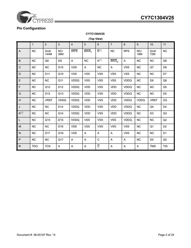
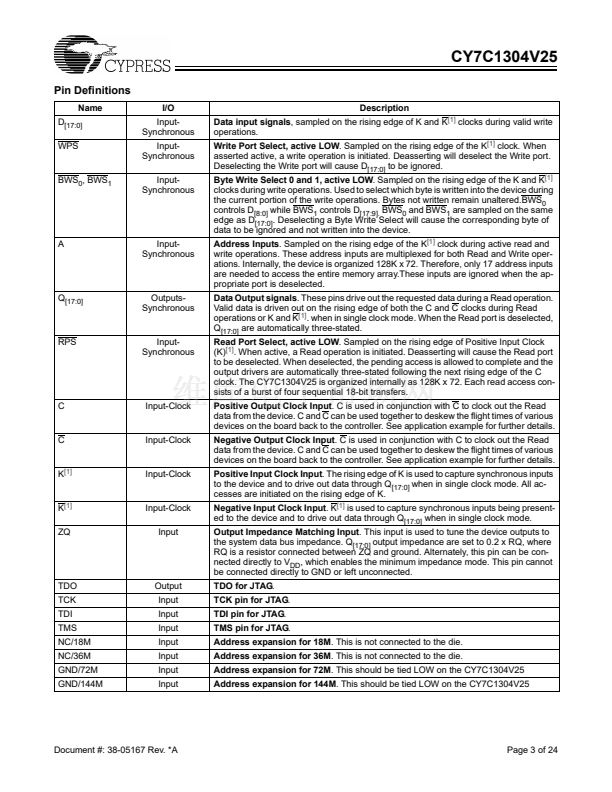
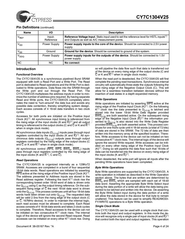
CY7C1304V25
9-Mb Pipelined SRAM with QDR鈩?Architecture
Features
鈥?Separate independent Read and Write data ports
鈥?Supports concurrent transactions
鈥?167 MHz Clock for high bandwidth
鈥?2.5 ns Clock-to-Valid access time
鈥?4-Word burst for reducing address bus frequency
鈥?Double Data Rate (DDR) interfaces on both Read & Write
Ports (data transferred at 333 MHz) @167 MHz
鈥?Two input clocks (K and K)
[1]
for precise DDR timing
鈥?SRAM uses rising edges only
鈥?Two output clocks (C and C) accounts for clock skew
and flight time mis-matches
鈥?Single multiplexed address input bus latches address
inputs for both READ and WRITE ports
鈥?Separate Port Selects for depth expansion
鈥?Synchronous internally self-timed writes
鈥?2.5V core power supply with HSTL Inputs and Outputs
[1]
鈥?13x15 mm 1.0 mm pitch fBGA package, 165 ball (11x15
matrix)
鈥?Variable drive HSTL output buffers
鈥?Expanded HSTL output voltage (1.4V-1.9V)
鈥?JTAG Interface
Functional Description
The CY7C1304V25 is a 2.5V Synchronous Pipelined SRAM
equipped with QDR architecture. QDR architecture consists of
two separate ports to access the memory array. The Read port
has dedicated Data Outputs to support Read operations and
the Write Port has dedicated Data Inputs to support Write op-
erations. QDR architecture has separate data inputs and data
outputs to completely eliminate the need to 鈥渢urn-around鈥?the
data bus required with common I/O devices. Access to each
port is accomplished through a common address bus. Ad-
dresses for Read and Write addresses are latched on alter-
nate rising edges of the input (K)
[1]
clock. Accesses to the
CY7C1304V25 Read and Write ports are completely indepen-
dent of one another. In order to maximize data throughput,
both Read and Write ports are equipped with Double Data
Rate (DDR) interfaces. Each address location is associated
with 4 18-bit words that burst sequentially into or out of the
device. Since data can be transferred into and out of the de-
vice on every rising edge of both input clocks (K/K
[1]
and C/C)
memory bandwidth is maximized while simplifying system de-
sign by eliminating bus 鈥渢urn-arounds鈥?
Depth expansion is accomplished with Port Selects for each
port. Port selects allow each port to operate independently.
All synchronous inputs pass through input registers controlled
by the K or K
[1]
input clocks. Data outputs pass through output
registers controlled by the C or C input clocks. Writes are con-
ducted with on-chip synchronous self-timed write circuitry.
Logic Block Diagram
D
[17:0]
18
Write Write Write Write
Reg Reg Reg
Reg
Read Add. Decode
Write Add. Decode
A
(16:0)
Address
Register
17
128Kx18 Array
128Kx18 Array
128Kx18 Array
128Kx18 Array
Address
Register
17
A
(16:0)
K
[1]
K
[1]
CLK
Gen.
Control
Logic
RPS
C
C
Read Data Reg.
72
Control
Logic
36
Reg.
36
Reg.
18
Reg.
Vref
WPS
BWS
[0:1]
18
Q
[17:0]
Selection Guide
7C1304V25-167
Maximum Operating Frequency (MHz)
Maximum Operating Current (mA)
167
450
7C1304V25-133
133
350
7C1304V25-100
100
230
Note:
1. K and K inputs require V
IH
to be greater than V
REF
+ 0.5V and V
IL
to be less than V
REF
- 0.5. This is a subset of JEDEC standards for HSTL I/Os.
Cypress Semiconductor Corporation
Document #: 38-05167 Rev. *A
鈥?/div>
3901 North First Street
鈥?/div>
San Jose
鈥?/div>
CA 95134 鈥?408-943-2600
Revised August 15, 2002


 1
1
 2
2
 3
3
 4
4
 5
5
 6
6
 7
7
 8
8
 9
9
 10
10
 11
11
 12
12
 13
13
 14
14
 15
15
 16
16
 17
17
 18
18
 19
19
 20
20
 21
21
 22
22
 23
23
 24
24
