鈥?/div>
Fast clock speed: 100 and 83 MHz
Fast Access Times: 5.0/6.0 ns Max.
Single Clock Operation
Single 3.3V 鈥?% and +5% power supply VCC
Separate V
CCQ
for output buffer
Two chip enables for simple depth expansion
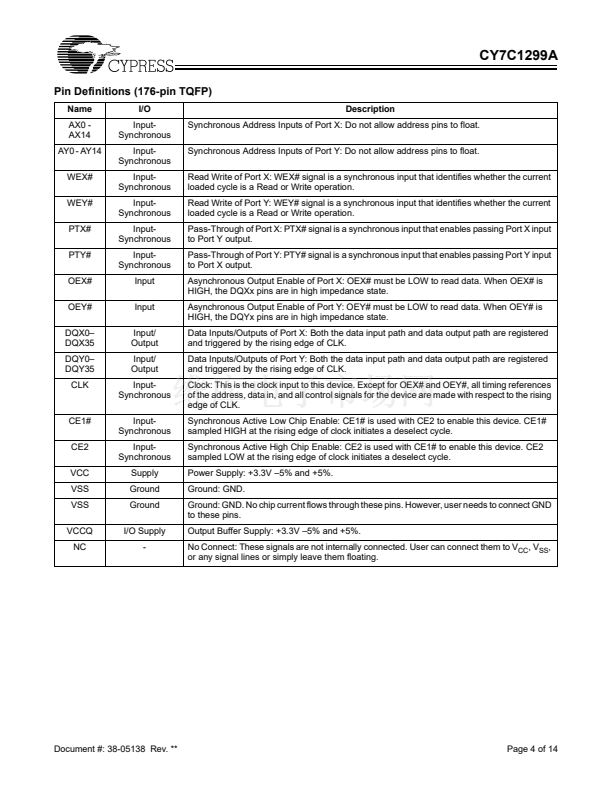
Address, Data Input, CE1#, CE2, PTX#, PTY#, WEX#,
WEY#, and Data Output Registers On-Chip
Concurrent Reads and Writes
Two Bidirectional Data Buses
Can be configured as separate I/O
Pass-Through Feature
Asynchronous Output Enables (OEX#, OEY#)
LVTTL Compatible I/O
Self-Timed Write
Automatic power down
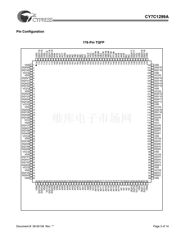
176-Pin TQFP Package
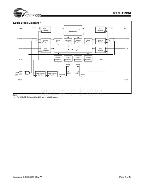
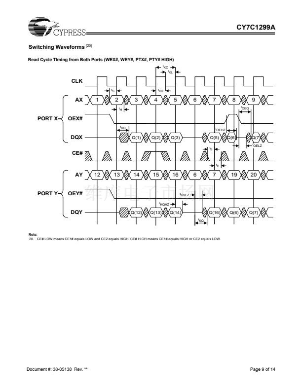
The CY7C1299A allows the user to concurrently perform
reads, writes, or pass-through cycles in combination on the
two data ports. The two address ports (AX, AY) determine the
read or write locations for their respective data ports (DQX,
DQY).
All input pins except output enable pins (OEX#, OEY#) are
gated by registers controlled by a positive-edge-triggered
clock input (CLK). The synchronous inputs include all address-
es, all data inputs, depth-expansion chip enables (CE1#,
CE2), pass-through controls (PTX# and PTY#), and read-write
control (WEX# and WEY#). The pass-through feature allows
data to be passed from one port to the other, in either direction.
The PTX# input must be asserted to pass data from port X to
port Y. The PTY# will likewise pass data from port Y to port X.
A pass-through operation takes precedence over a read oper-
ation.
For the case when AX and AY are the same, certain protocols
are followed. If both ports are read, the reads occur normally.
If one port is written and the other is read, the read from the
array will occur before the data is written. If both ports are
written, only the data on DQY will be written to the array.
The CY7C1299A operates from a +3.3V power supply. All in-
puts and outputs are LVTTL compatible. These dual I/O, dual
address synchronous SRAMs are well suited for ATM, Ether-
net switches, routers, cell/frame buffers, SNA switches and
shared memory applications.
The CY7C1299A needs one extra cycle after power for proper
power-on reset. The extra cycle is needed after V
CC
is stable
on the device.
This device is available in a 176-pin TQFP package.
Functional Description
The CY7C1299A SRAM integrates 32,768 x 36 SRAM cells
with advanced synchronous peripheral circuitry. It employs
high-speed, low-power CMOS designs using advanced tri-
ple-layer polysilicon, double-layer metal technology. Each
memory cell consists of four transistors and two high valued
resistors.
Selection Guide
-100
Maximum Access Time (ns)
Maximum Operating Current (mA)
Maximum CMOS Standby Current (mA)
5.0
350
100
-83
6.0
300
100
Cypress Semiconductor Corporation
Document #: 38-05138 Rev. **
鈥?/div>
3901 North First Street
鈥?/div>
San Jose
鈥?/div>
CA 95134 鈥?408-943-2600
Revised October 9, 2001


 1
1
 2
2
 3
3
 4
4
 5
5
 6
6
 7
7
 8
8
 9
9
 10
10
 11
11
 12
12
 13
13
 14
14
