鈥?/div>
Function, pinout, and drive compatible with FCT, F, and
AM29827 logic
鈥?FCT-C speed at 4.4 ns max. (Com鈥檒)
FCT-A speed at 5.0 ns max. (Com鈥檒)
鈥?Reduced V
OH
(typically = 3.3V) versions of equivalent
FCT functions
鈥?Edge-rate control circuitry for signi鏗乧antly improved
noise characteristics
鈥?Power-off disable feature
鈥?/div>
ESD > 2000V
鈥?Matched rise and fall times
鈥?Fully compatible with TTL input and output logic levels
Functional Description
The FCT827T 10-bit bus driver provides high-performance
bus interface buffering for wide data/address paths or buses
carrying parity. The 10-bit buffers have NAND-ed output
enables for maximum control 鏗俥xibility. The FCT827T is
designed for high-capacitance load drive capability, while providing
low-capacitance bus loading at both inputs and outputs. All outputs
are designed for low-capacitance bus loading in the
high-impedance state and are designed with a power-off disable
feature to allow for live insertion of boards.
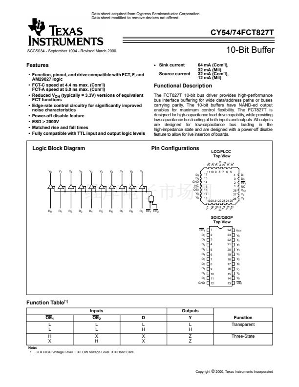
Logic Block Diagram
Pin Configurations
LCC/PLCC
Top View
D7
D6
D5
NC
D4
D3
D2
D
1
D
0
OE
1
NC
V
CC
Y
0
Y
1
24
23
22
21
20
19
18
17
16
15
14
13
V
CC
Y
0
Y
1
Y
2
Y
3
Y
4
Y
5
Y
6
Y
7
Y
8
Y
9
OE
2
Y
0
Y
1
Y
2
Y
3
Y
4
Y
5
Y
6
Y
7
Y
8
Y
9
D
8
D
9
GND
NC
OE
2
Y
9
Y
8
11 10 9 8 7 6 5
12
4
13
3
14
2
1
15
16
28
17
27
18
26
19 20 21 22 23 24 25
Y7
Y6
Y5
NC
Y4
Y3
Y2
D
0
D
1
D
2
D
3
D
4
D
5
D
6
D
7
D
8
D
9
OE
1
OE
2
SOIC/QSOP
Top View
OE
1
D
0
D
1
D
2
D
3
D
4
D
5
D
6
D
7
D
8
D
9
GND
1
2
3
4
5
6
7
8
9
10
11
12
Function Table
[1]
Inputs
OE
1
L
L
H
X
OE
2
L
L
X
H
D
L
H
X
X
Outputs
Y
L
H
Z
Z
Function
Transparent
Three-State
Note:
1. H = HIGH Voltage Level. L = LOW Voltage Level. X = Don鈥檛 Care
Copyright
漏
2000, Texas Instruments Incorporated


 1
1
 2
2
 3
3
 4
4
 5
5
 6
6
 7
7
