Data sheet acquired from Cypress Semiconductor Corporation.
Data sheet modi鏗乪d to remove devices not offered.
CY54/74FCT646T
SCCS031 - July 1994 - Revised March 2000
8-Bit Registered Transceiver
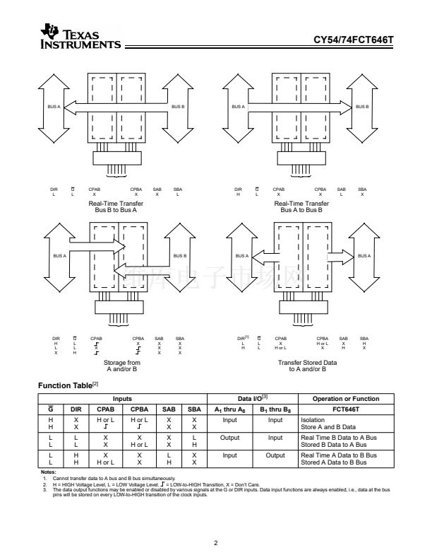
Functional Description
The FCT646T consists of a bus transceiver circuit with
three-state, D-type 鏗俰p-鏗俹ps, and control circuitry arranged for
multiplexed transmission of data directly from the input bus or
from the internal registers. Data on the A or B bus will be
clocked into the registers as the appropriate clock pin goes to
a HIGH logic level. Enable Control G and direction pins are
provided to control the transceiver function. In the transceiver
mode, data present at the high-impedance port may be stored
in either the A or B register, or in both. The select controls can
multiplex stored and real-time (transparent mode) data. The
direction control determines which bus will receive data when
the enable control G is Active LOW. In the isolation mode
(enable Control G HIGH), A data may be stored in the B reg-
ister and/or B data may be stored in the A register.
The outputs of the FCT646T are designed with a power-off
disable feature to allow for live insertion of boards.
Features
鈥?Function, pinout, and drive compatible with FCT and
F logic
鈥?FCT-C speed at 5.4 ns max. (Com鈥檒)
FCT-A speed at 6.3 ns max. (Com鈥檒)
鈥?Reduced V
OH
(typically = 3.3V) versions of equivalent
FCT functions
鈥?Edge-rate control circuitry for signi鏗乧antly improved
noise characteristics
鈥?Power-off disable feature permits live insertion
鈥?Matched rise and fall times
鈥?Fully compatible with TTL input and output logic levels
鈥?ESD > 2000V
鈥?Sink current
64 mA (Com鈥檒), 48 mA (Mil)
Source current
32 mA (Com鈥檒), 12 mA (Mil)
鈥?Independent register for A and B buses
鈥?Extended commercial range of
鈭?0藲C
to +85藲C
Function Block Diagrams
G
Pin Configurations
LCC
Top View
A6
A5
A4
NC
A3
A2
A1
CPAB
SAB
A
7
A
8
GND
NC
B
8
B
7
B
6
11 10 9 8 7 6 5
12
4
3
13
2
14
1
15
16
28
27
17
18
26
19 20 21 22 23 24 25
B5
B4
B3
NC
B2
B1
G
DIR
SAB
CPAB
NC
V
CC
CPBA
SBA
DIR
A
1
A
2
A
3
A
4
A
5
A
6
A
7
A
8
GND
B
1
QSOP, SOIC
Top View
1
2
3
4
5
6
7
8
9
10
11
12
24
23
22
21
20
19
18
17
16
15
14
13
V
CC
CPBA
SBA
G
B
1
B
2
B
3
B
4
B
5
B
6
B
7
B
8
DIR
CPBA
SBA
CPAB
SAB
D
C
A
1
D
C
Logic Block Diagram
A
1
CPAB
SAB
DIR
CPBA
SBA
G
B
1
B
2
B
3
B
4
B
5
B
6
B
7
B
8
A
2
A
3
A
4
A
5
A
6
A
7
A
8
TO 7 OTHER CHANNELS
Pin Description
Name
A
B
CPAB, CPBA
SAB, SBA
DIR, G
Description
Data Register A Inputs, Data Register B Outputs
Data Register B Inputs, Data Register A Outputs
Clock Pulse Inputs
Output Data Source Select Inputs
Output Enable Inputs
Copyright
漏
2000, Texas Instruments Incorporated


 1
1
 2
2
 3
3
 4
4
 5
5
 6
6
 7
7
 8
8
