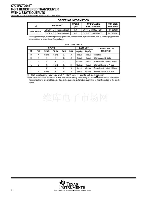
CY74FCT2646T
8-BIT REGISTERED TRANSCEIVER
WITH 3-STATE OUTPUTS
SCCS043C 鈥?SEPTEMBER 1994 鈥?REVISED NOVEMBER 2001
D
D
D
D
D
D
D
D
D
D
D
Function and Pinout Compatible With FCT
and F Logic
Reduced V
OH
(Typically = 3.3 V) Versions
of Equivalent FCT Functions
25-鈩?Output Series Resistors to Reduce
Transmission-Line Reflection Noise
Edge-Rate Control Circuitry for
Significantly Improved Noise
Characteristics
I
off
Supports Partial-Power-Down Mode
Operation
Matched Rise and Fall Times
ESD Protection Exceeds JESD 22
鈥?2000-V Human-Body Model (A114-A)
鈥?200-V Machine Model (A115-A)
鈥?1000-V Charged-Device Model (C101)
Fully Compatible With TTL Input and
Output Logic Levels
12-mA Output Sink Current
15-mA Output Source Current
Independent Register for A and B Buses
3-State Outputs
Q PACKAGE
(TOP VIEW)
CPAB
SAB
DIR
A
1
A
2
A
3
A
4
A
5
A
6
A
7
A
8
GND
1
2
3
4
5
6
7
8
9
10
11
12
24
23
22
21
20
19
18
17
16
15
14
13
V
CC
CPBA
SBA
G
B
1
B
2
B
3
B
4
B
5
B
6
B
7
B
8
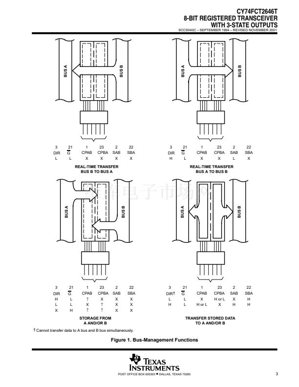
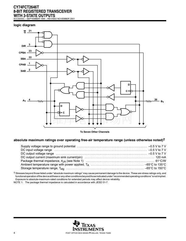
description
The CY74FCT2646T consists of a bus transceiver circuit with 3-state, D-type flip-flops, and control circuitry
arranged for multiplexed transmission of data directly from the input bus or from the internal registers. Data on
the A or B bus is clocked into the registers as the appropriate clock pin goes to a high logic level.
Output-enable (G) and direction-control (DIR) inputs determine the transceiver function. On-chip termination
resistors at the outputs reduce system noise caused by reflections, so that the CY74FCT2646T can replace
the CY74FCT646T in an existing design.
In the transceiver mode, data present at the high-impedance port can be stored in either the A or B register,
or in both. Select controls (SAB, SBA) can multiplex stored and real-time (transparent mode) data. DIR
determines which bus receives data when G is active low. In the isolation mode (G is high), A data can be stored
in the B register and/or B data can be stored in the A register.
This device is fully specified for partial-power-down applications using I
off
. The I
off
circuitry disables the outputs,
preventing damaging current backflow through the device when it is powered down.
PIN DESCRIPTION
NAME
A
B
CPAB, CPBA
SAB, SBA
DIR, G
DESCRIPTION
Data register A inputs, data register B outputs
Data register B inputs, data register A outputs
Clock pulse inputs
Output data source select inputs
Output-enable inputs
Please be aware that an important notice concerning availability, standard warranty, and use in critical applications of
Texas Instruments semiconductor products and disclaimers thereto appears at the end of this data sheet.
Copyright
錚?/div>
2001, Texas Instruments Incorporated
PRODUCTION DATA information is current as of publication date.
Products conform to specifications per the terms of Texas Instruments
standard warranty. Production processing does not necessarily include
testing of all parameters.
POST OFFICE BOX 655303
鈥?/div>
DALLAS, TEXAS 75265
1


 1
1
 2
2
 3
3
 4
4
 5
5
 6
6
 7
7
 8
8
 9
9
