Data sheet acquired from Cypress Semiconductor Corporation.
Data sheet modi鏗乪d to remove devices not offered.
CY74FCT16823T
CY74FCT162823T
SCCS062B - August 1994 - Revised September 2001
18-Bit Registers
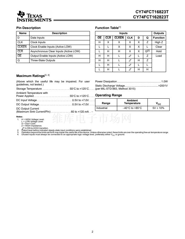
Functional Description
The CY74FCT16823T and the CY74FCT162823T 18-bit bus
interface registers are designed for use in high-speed,
low-power systems needing wide registers and parity. 18-bit
operation is achieved by connecting the control lines of the two
9-bit registers. Flow-through pinout and small shrink
packaging aids in simplifying board layout.
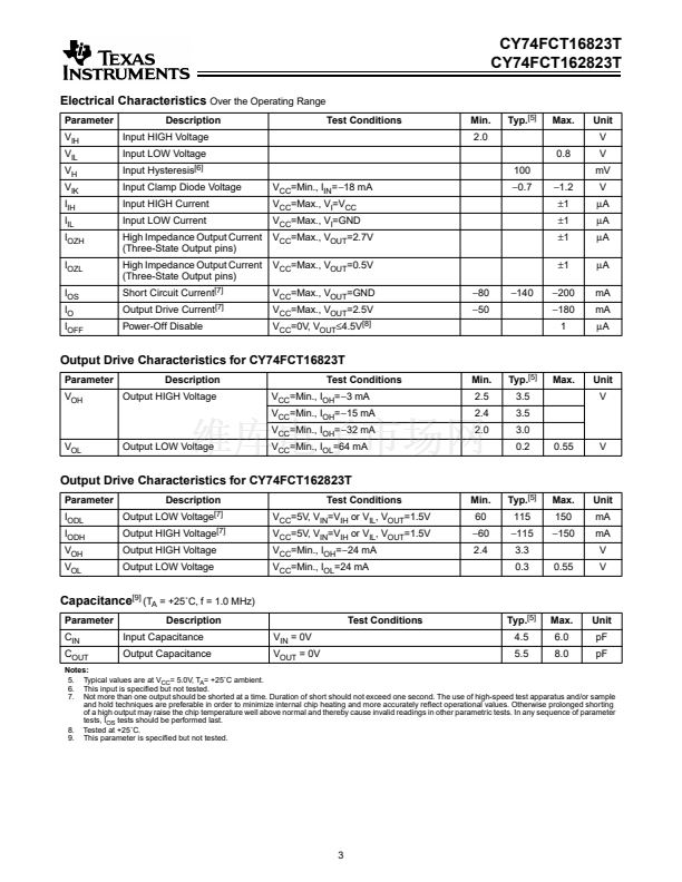
This device is fully speci鏗乪d for partial-power-down
applications using I
off
. The I
off
circuitry disables the outputs,
preventing damaging current back鏗俹w through the device
when it is powered down.
The CY74FCT16823T is ideally suited for driving
high-capacitance loads and low-impedance backplanes.
The CY74FCT162823T has 24-mA balanced output drivers
with current limiting resistors in the outputs. This reduces the
need for external terminating resistors and provides for
minimal undershoot and reduced ground bounce. The
CY74FCT162823T is ideal for driving transmission lines.
Features
鈥?I
off
supports partial-power-down mode operation
鈥?Edge-rate control circuitry for signi鏗乧antly improved
noise characteristics
鈥?Typical output skew < 250 ps
鈥?ESD > 2000V
鈥?TSSOP (19.6-mil pitch) and SSOP (25-mil pitch)
packages
鈥?Industrial temperature range of
鈭?0藲C
to +85藲C
鈥?V
CC
= 5V
鹵
10%
CY74FCT16823T Features:
鈥?64 mA sink current, 32 mA source current
鈥?Typical V
OLP
(ground bounce) <1.0V at V
CC
= 5V,
T
A
= 25藲C
CY74FCT162823T Features:
鈥?Balanced 24 mA output drivers
鈥?Reduced system switching noise
鈥?/div>
Typical V
OLP
(ground bounce) <0.6V at V
CC
= 5V,
TA = 25藲C
Logic Block Diagrams
1
OE
1
CLR
Pin Configuration
SSOP/TSSOP
Top View
1
CLR
1
2
3
4
5
6
7
8
9
10
11
12
13
14
15
16
17
18
19
20
21
22
23
24
25
26
27
28
56
55
54
53
52
51
50
49
48
47
46
45
44
43
42
41
40
39
38
37
36
35
34
33
32
31
30
29
1
CLK
1
CLKEN
1
D
1
1
CLK
1
OE
1
Q
1
1
CLKEN
GND
1
Q
2
1
Q
3
GND
1
D
2
1
D
3
V
CC
R
C
D
1
D
1
1
Q
4
1
Q
1
1
Q
5
1
Q
6
V
CC
1
D
4
1
D
5
1
D
6
GND
1
Q
7
1
Q
8
GND
1
D
7
1
D
8
1
D
9
2
D
1
2
D
2
2
D
3
FCT16823-1
TO 8 OTHER CHANNELS
2
OE
1
Q
9
2
Q
1
2
Q
2
2
Q
3
2
CLR
GND
2
Q
4
2
Q
5
2
Q
6
GND
2
D
4
2
D
5
2
D
6
2
CLK
2
CLKEN
V
CC
2
Q
7
2
Q
8
V
CC
2
D
7
2
D
8
R
C
D
2
D
2
GND
2
Q
1
2
Q
9
2
OE
2
CLR
GND
2
D
9
2
CLKEN
2
CLK
TO 8 OTHER CHANNELS
FCT16823-2
FCT16823-3
Copyright
漏
2001, Texas Instruments Incorporated


 1
1
 2
2
 3
3
 4
4
 5
5
 6
6
 7
7
 8
8
