CY62137V MoBL鈩?/div>
128K x 16 Static RAM
Features
鈥?Low voltage range:
鈥?CY62137V: 2.7V鈥?.6V
鈥?Ultra-low active, standby power
鈥?Easy memory expansion with CE and OE features
鈥?TTL-compatible inputs and outputs
鈥?Automatic power-down when deselected
鈥?CMOS for optimum speed/power
high-impedance state when: deselected (CE HIGH), outputs
are disabled (OE HIGH), BHE and BLE are disabled (BHE,
BLE HIGH), or during a write operation (CE LOW, and WE
LOW).
Writing to the device is accomplished by taking Chip Enable
(CE) and Write Enable (WE) inputs LOW. If Byte Low Enable
(BLE) is LOW, then data from I/O pins (I/O
0
through I/O
7
), is
written into the location specified on the address pins (A
0
through A
16
). If Byte High Enable (BHE) is LOW, then data
from I/O pins (I/O
8
through I/O
15
) is written into the location
specified on the address pins (A
0
through A
16
).
Reading from the device is accomplished by taking Chip
Enable (CE) and Output Enable (OE) LOW while forcing the
Write Enable (WE) HIGH. If Byte Low Enable (BLE) is LOW,
then data from the memory location specified by the address
pins will appear on I/O
0
to I/O
7
. If Byte High Enable (BHE) is
LOW, then data from memory will appear on I/O
8
to I/O
15
. See
the truth table at the back of this data sheet for a complete
description of read and write modes.
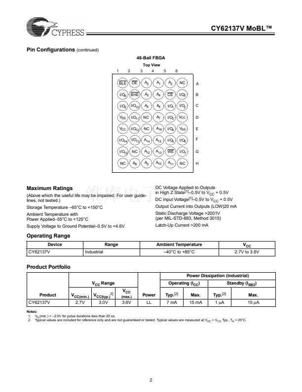
The CY62137V is available in 48-ball FBGA and standard
44-pin TSOP Type II (forward pinout) packaging.
Functional Description
The CY62137V is a high-performance CMOS static RAM or-
ganized as 131,072 words by 16 bits. This device features ad-
vanced circuit design to provide ultra-low active current. This
is ideal for providing More Battery Life鈩?(MoBL鈩? in portable
applications such as cellular telephones. The device also has
an automatic power-down feature that reduces power con-
sumption by 99% when addresses are not toggling. The device
can also be put into standby mode when deselected (CE
HIGH) or when CE is LOW and both BLE and BHE are HIGH.
The input/output pins (I/O
0
through I/O
15
) are placed in a
Logic Block Diagram
Pin Configurations
TSOP II (Forward)
Top View
DATA IN DRIVERS
A
9
A
8
A
7
A
6
A
5
A
4
A
3
A
2
A
1
A
0
128K x 16
RAM Array
I/O
0
鈥揑/O
7
I/O
8
鈥揑/O
15
COLUMN DECODER
BHE
WE
CE
OE
BLE
CE
BHE
BLE
Power Down
Circuit
MoBL and More Battery Life are trademarks of Cypress Semiconductor Corporation.
Cypress Semiconductor Corporation
A
10
A
11
A
12
A
13
A
14
A
15
A
16
A
4
A
3
A
2
A
1
A
0
CE
I/O
0
I/O
1
I/O
2
I/O
3
V
CC
V
SS
I/O
4
I/O
5
I/O
6
I/O
7
WE
A
16
A
15
A
14
A
13
A
12
1
2
3
4
5
6
7
8
9
10
11
12
13
14
15
16
17
18
19
20
21
22
44
43
42
41
40
39
38
37
36
35
34
33
32
31
30
29
28
27
26
25
24
23
A
5
A
6
A
7
OE
BHE
BLE
I/O
15
I/O
14
I/O
13
I/O
12
V
SS
V
CC
I/O
11
I/O
10
I/O
9
I/O
8
NC
A
8
A
9
A
10
A
11
NC
ROW DECODER
鈥?/div>
SENSE AMPS
3901 North First Street
鈥?/div>
San Jose
鈥?/div>
CA 95134
鈥?/div>
408-943-2600
February 2, 2001


 1
1
 2
2
 3
3
 4
4
 5
5
 6
6
 7
7
 8
8
 9
9
 10
10
 11
11
