鈥?/div>
Very high speed: 55 and 70 ns
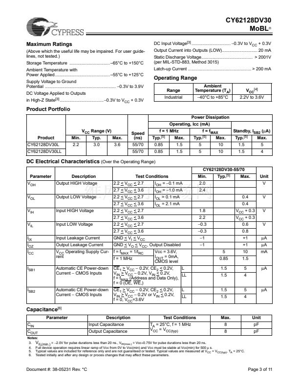
Wide voltage range: 2.2V to 3.6V
Pin compatible with CY62128V
Ultra-low active power
鈥?Typical active current: 0.85 mA @ f = 1 MHz
鈥?Typical active current: 5 mA @ f = f
MAX
Ultra-low standby power
Easy memory expansion with CE
1
, CE
2
, and OE
features
Automatic power-down when deselected
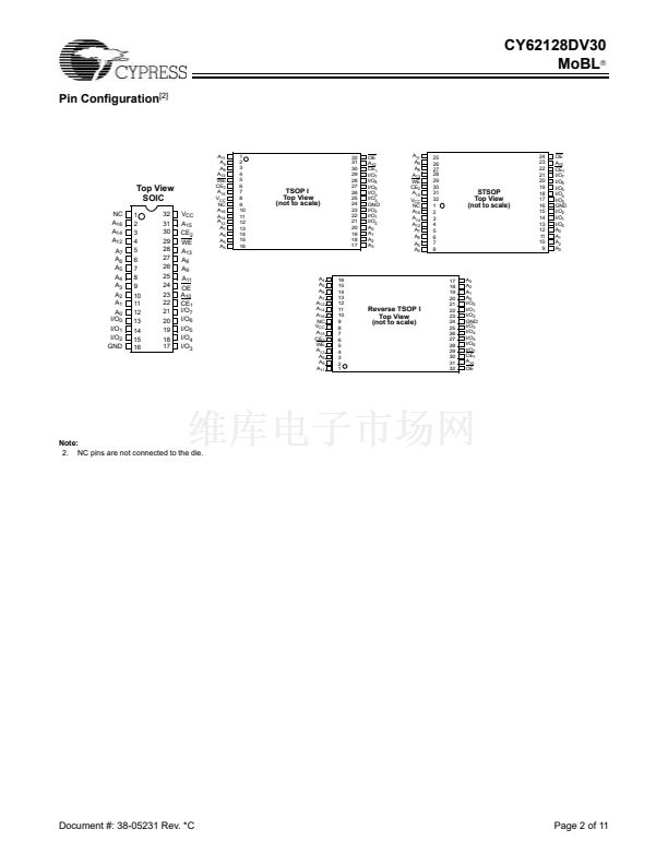
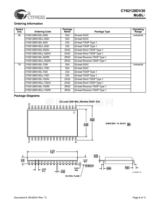
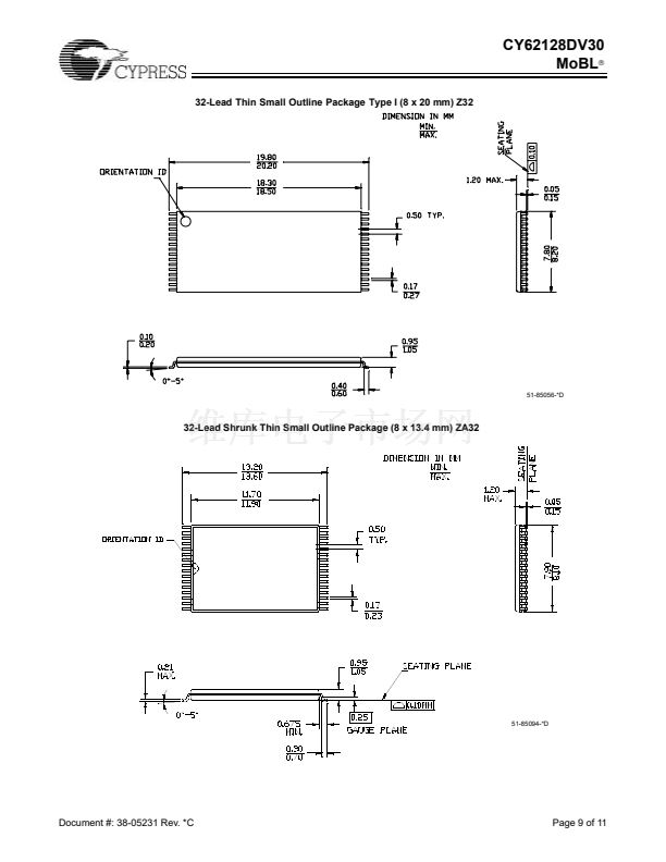
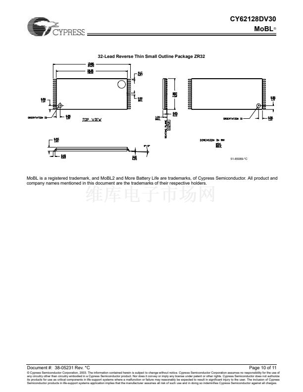
Packages offered in a 32-lead SOIC, a 32-lead TSOP, a
32-lead Short TSOP, and a 32-lead Reverse TSOP
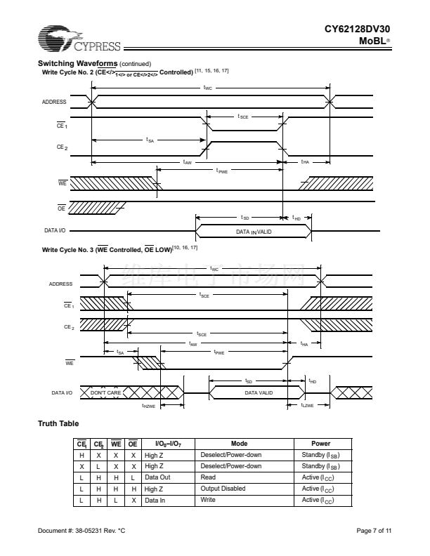
power consumption by 90% when addresses are not toggling.
The device can be put into standby mode reducing power con-
sumption by more than 99% when deselected Chip Enable 1
(CE
1
) HIGH or Chip Enable 2 (CE
2
) LOW. The input/output
pins (I/O
0
through I/O
7
) are placed in a high-impedance state
when: deselected Chip Enable 1 (CE
1
) HIGH or Chip Enable
2 (CE
2
) LOW, outputs are disabled (OE HIGH), or during a
write operation (Chip Enable 1 (CE
1
) LOW and Chip Enable 2
(CE
2
) HIGH and Write Enable (WE) LOW).
Writing to the device is accomplished by taking Chip Enable 1
(CE
1
) LOW with Chip Enable 2 (CE
2
) HIGH and Write En-
able(WE) LOW. Data on the eight I/O pins is then written into
the location specified on the Address pin (A
0
thro. A
16
).
Reading from the device is accomplished by taking Chip En-
able 1 (CE
1
) LOW with Chip Enable 2 (CE
2
) HIGH and Output
Enable (OE) LOW while forcing the Write Enable (WE) HIGH.
Under these conditions, the contents of the memory location
specified by the address pins will appear on the I/O pins.
The eight input/output pins (I/O
o
through I/O
7
) are placed in a
high-impedance state when the device is deselected (CE
1
HIGH or CE
2
LOW), the outputs are disabled (OE HIGH) or
during a write operation (CE
1
LOW, CE
2
HIGH), and WE
LOW).
鈥?/div>
鈥?/div>
鈥?/div>
鈥?/div>
Functional Description
[1]
The CY62128DV30 is a high-performance CMOS static RAM
organized as 128K words by 8 bits. This device features ad-
vanced circuit design to provide ultra-low active current. This
is ideal for providing More Battery Life錚?(MoBL
廬
) in portable
applications such as cellular telephones. The device also has
an automatic power-down feature that significantly reduces
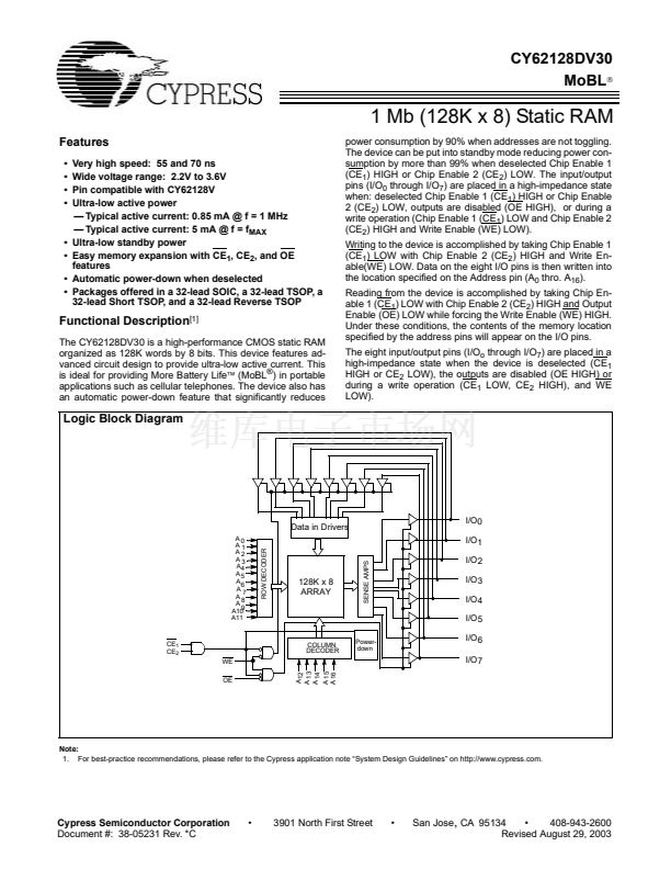
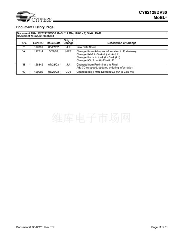
Logic Block Diagram
Data in Drivers
A0
A1
A2
A3
A4
A5
A
6
A7
A8
A
9
A10
A11
ROW DECODER
I/O0
I/O1
SENSE AMPS
I/O 2
I/O 3
I/O 4
I/O 5
128K x 8
ARRAY
CE
1
CE
2
WE
COLUMN
DECODER
Power-
down
I/O 6
I/O 7
A 12
A 13
A 14
OE
Note:
1. For best-practice recommendations, please refer to the Cypress application note 鈥淪ystem Design Guidelines鈥?on http://www.cypress.com.
A 15
A 16
Cypress Semiconductor Corporation
Document #: 38-05231 Rev. *C
鈥?/div>
3901 North First Street
鈥?/div>
San Jose
,
CA 95134
鈥?/div>
408-943-2600
Revised August 29, 2003
CY62128DV30L-70ZRI相關(guān)型號(hào)PDF文件下載
-
型號(hào)
版本
描述
廠商
下載
-
英文版
8K x 8 Static RAM
Cypress
-
英文版
128K x 8 Static RAM
CYPRESS
-
英文版
128K x 8 Static RAM
CYPRESS [C...
-
英文版
512K x 8 MoBL Static RAM
CYPRESS
-
英文版
512K x 8 MoBL Static RAM
CYPRESS [C...
-
英文版
32Kx8 Static RAM
Cypress
-
英文版
64K x 16 Static RAM
Cypress
-
英文版
64K x 16 Static RAM
Cypress
-
英文版
128K x 8 Static RAM
CYPRESS
-
英文版
128K x 8 Static RAM
CYPRESS [C...
-
英文版
1-Mbit (128K x 8) Static RAM
CYPRESS [C...
-
英文版
128K x 8 Static RAM
CYPRESS
-
英文版
128K x 8 Static RAM
CYPRESS [C...
-
英文版
128K x 16 Flash Compatible Static RAM
Cypress
-
英文版
Memory
ETC
-
英文版
128K x 16 Static RAM
Cypress
-
英文版
2-Mbit (128K x 16) Static RAM
CYPRESS
-
英文版
2-Mbit (128K x 16) Static RAM
CYPRESS [C...
-
英文版
Cypress Semiconductor [2-Mbit (256K x 8) Static RAM]
CYPRESS
-
英文版
256K x 8 Static RAM
CYPRESS


 1
1
 2
2
 3
3
 4
4
 5
5
 6
6
 7
7
 8
8
 9
9
 10
10
 11
11
