ADVANCE
INFORMATION
CY62127DV18
MoBL2
廬
1M
(64K x
16)
Static RAM
Features
鈥?Very high
speed:
55 ns
鈥?Voltage
range:
1.65V
to
1.95V
鈥?Ultra-low active power
鈥?Typical active current:
0.5
mA @ f = 1 MHz
鈥?Typical active current:
2.5
mA @ f = f
MAX
鈥?Ultra-low standby power
鈥?Easy memory expansion with
CE
1
, CE
2
and OE features
鈥?Automatic power-down when deselected
鈥?CMOS for optimum speed/power
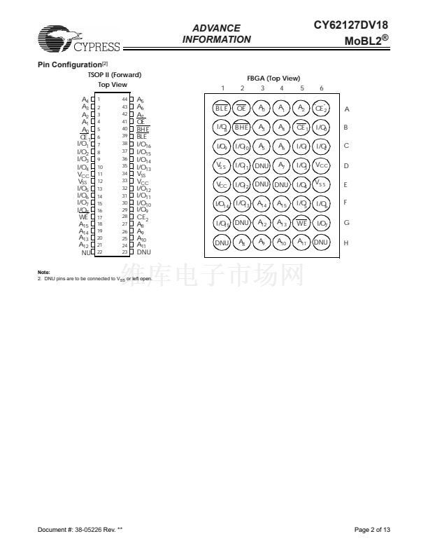
鈥?Packages offered in a 48-ball FBGA and a 44-pin TSOP
Type II
BLE are HIGH. The input/output pins (I/O
0
through I/O
15
) are
placed in a high-impedance state when: deselected
Chip En-
able 1 (CE
1
) HIGH or Chip Enable 2 (CE
2
) LOW, outputs are
disabled (OE HIGH),
both Byte High Enable and Byte Low
Enable are disabled (BHE,
BLE HIGH) or during a write oper-
ation (Chip
Enable 1 (CE
1
) LOW and Chip Enable 2 (CE
2
)
HIGH and WE LOW).
Writing to the device is accomplished by taking Chip Enable 1
(CE
1
) LOW and Chip Enable 2 (CE
2
) HIGH and Write Enable
(WE) input LOW. If Byte Low Enable (BLE) is LOW, then data
from I/O pins (I/O
0
through I/O
7
), is written into the location
specified on the address
pins (A
0
through A
15
). If Byte High
Enable (BHE) is LOW, then data from I/O pins (I/O
8
through
I/O
15
) is written into the location specified on the address pins
(A
0
through A
15
).
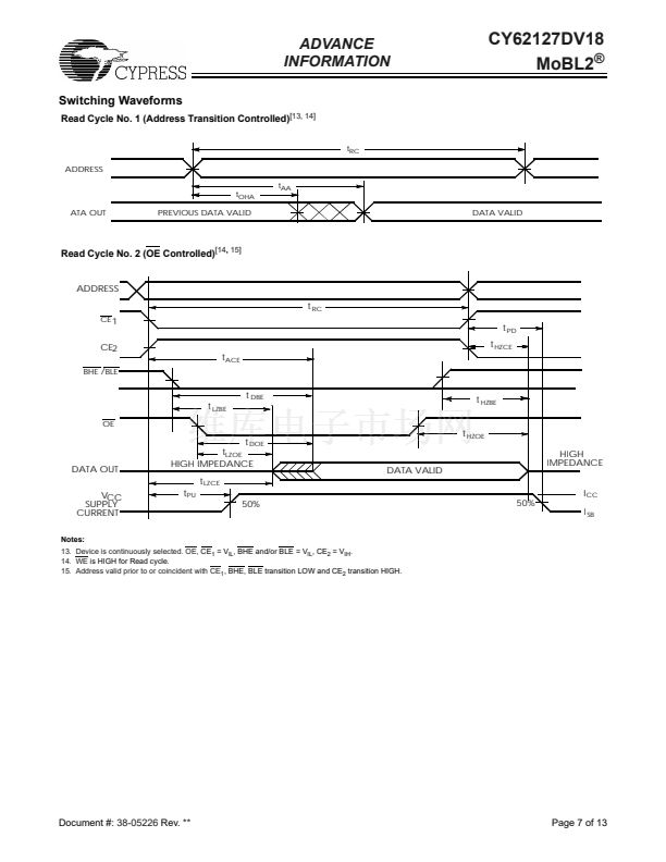
Reading from the device is accomplished by taking Chip En-
able 1 (CE
1
) LOW and Chip Enable 2 (CE
2
) HIGH and Output
Enable (OE) LOW while forcing the Write Enable (WE) HIGH.
If Byte Low Enable (BLE) is LOW, then data from the memory
location specified by the address pins will appear on I/O
0
to
I/O
7
. If Byte High Enable (BHE) is LOW, then data from mem-
ory will appear on I/O
8
to I/O
15
. See the truth table at the back
of this data sheet for a complete description of read and write
modes.
Functional Description
[1]
The CY62127DV18 is a high-performance CMOS static RAM
organized as 64K words by 16 bits. This device features
ad-
vanced circuit design to provide ultra-low active current. This
is ideal for providing More Battery Life錚?(MoBL
廬
) in portable
applications such as cellular telephones. The
device also
has
an automatic power-down feature that significantly reduces
power consumption by
99%
when addresses are not toggling.
The device can be put into standby mode reducing power con-
sumption by more than 99% when deselected
Chip Enable 1
(CE
1
) HIGH or Chip Enable 2 (CE
2
) LOW
or both BHE
and
Logic Block Diagram
DATA IN DRIVERS
A
10
A
9
A
8
A
7
A
6
A
5
A
4
A
3
A
2
A
1
A
0
ROW DECODER
64K 脳 16
RAM ARRAY
2048 x 32 x 16
SENSE AMPS
I/O
0
鈥揑/O
7
I/O
8
鈥揑/O
15
COLUMN DECODER
A
14
A
12
A
11
A
13
A
15
BHE
WE
OE
BLE
CE
2
CE
1
Power-down
Circuit
BHE
BLE
CE
2
CE
1
Note:
1. For best-practice recommendations, please refer to the Cypress application note 鈥淪ystem Design Guidelines鈥?on http://www.cypress.com.
Cypress Semiconductor Corporation
Document #:
38-05226
Rev.
**
鈥?/div>
3901 North First Street
鈥?/div>
San Jose
鈥?/div>
CA 95134 鈥?408-943-2600
Revised September 24, 2002


 1
1
 2
2
 3
3
 4
4
 5
5
 6
6
 7
7
 8
8
 9
9
 10
10
 11
11
 12
12
 13
13
