CY5057
High-Frequency Flash Programmable
PLL Die with Spread Spectrum
Features
鈥?Flash-programmable die for in-package programming
of crystal oscillators
Benefits
Enables quick turnaround of custom oscillators, and lowers
inventory costs through stocking blank parts. In addition, the
part can be programmed up to 100 times, which reduces
programming errors and provides an easy upgrade path for
existing designs
Enables synthesis of highly accurate and stable output clock
frequencies with zero or low PPM
Enables fine-tuning of output clock frequency by adjusting
C
Load
of the crystal
Allows the device to go into standard four- or six-pin packages.
Lowers cost of oscillator, as PLL can be programmed to a high
frequency using a low-frequency, low-cost crystal
Provides various spread percentage
Provides ability to enable or disable Spread Spectrum with an
external pin
Services most PC, networking, and consumer applications
Provides flexibility in output configurations and testing
Enables low-power operation or output enable function
Provides flexibility for system applications, through selectable
instantaneous or synchronous change in outputs
Suitable for most PC, consumer, and networking applications
Has lower EMI than oscillators
Easy-to-use software support for design entry
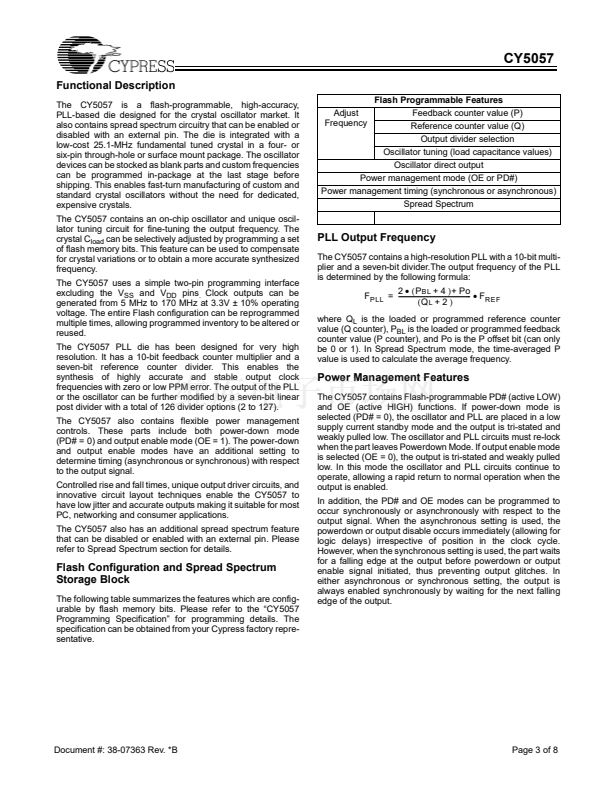
鈥?High-resolution phase-locked loop (PLL) with 10-bit
multiplier and seven-bit divider
鈥?Flash-programmable capacitor tuning array
鈥?Simple two-pin programming interface (excluding V
DD
and V
SS
pins)
鈥?On-chip oscillator used with external 25.1-MHz funda-
mental tuned crystal
鈥?Flash-programmable spread spectrum with spread
percentages between +0.25% and +2.00%
鈥?Spread Spectrum On/Off function
鈥?Operating frequency
5鈥?70 MHz at 3.3V 鹵 10%
鈥?Seven-bit linear post divider with divide options from
divide-by-2 to divide-by-127
鈥?Programmable PD# or OE pin
鈥?Programmable asynchronous or synchronous OE and
PD# modes
鈥?Low jitter output
< 200 ps (pk-pk) at 3.3V 鹵 10%
鈥?Controlled rise and fall times and output slew rate
鈥?Software Configuration Support
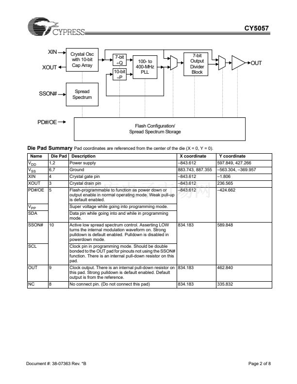
Die Pad Description
Horizontal scribe
1
VDD
2
VDD
SSON#
10
OUT
9
3
XOUT
Y
NC
8
Note:
Vertical scribe
4
XIN
5
PD#/OE
VSS
7
VSS
6
X
Active Die Size: X = 75.0 mils / 1907
碌m
Y = 56.2 mils / 1428
碌m
Scribe: X (horizontal)= 2.8 mils / 71
碌m
Y (vertical)= 3.4 mils / 86.2
碌m
Bond pad opening: 85
碌m
x 85
碌m
Pad pitch: 125
碌m
x 125
碌m
(Pad center to pad center)
Wafer thickness: 11 mils TYPICAL
Cypress Semiconductor Corporation
Document #: 38-07363 Rev. *B
鈥?/div>
3901 North First Street
鈥?/div>
San Jose
,
CA 95134
鈥?/div>
408-943-2600
Revised June 30,2003


 1
1
 2
2
 3
3
 4
4
 5
5
 6
6
 7
7
 8
8
