CY2SSTV857-27
Differential Clock Buffer/Driver
DDR333/PC2700-Compliant
Features
鈥?Operating frequency: 60 MHz to 200 MHz
鈥?Supports 266, 333-MHz DDR SDRAM
鈥?10 differential outputs from 1 differential input
鈥?Spread-Spectrum-compatible
鈥?Low jitter (cycle-to-cycle): < 75
鈥?Very low skew: < 100 ps
鈥?Power management control input
鈥?High-impedance outputs when input clock < 10 MHz
鈥?2.5V operation
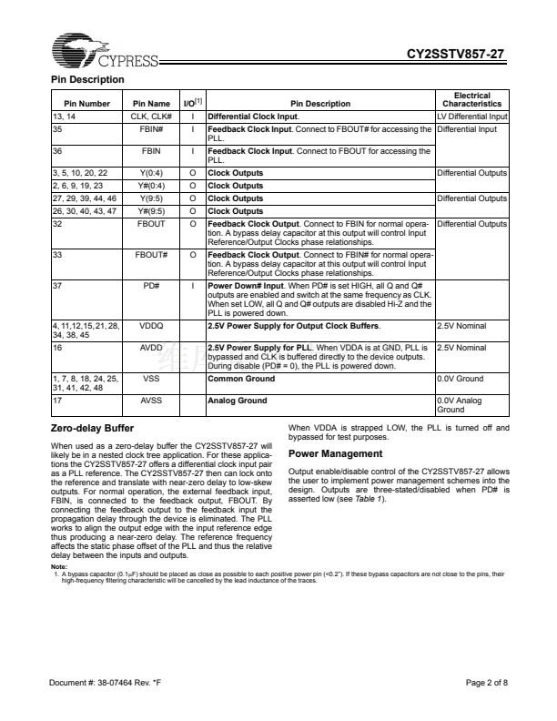
鈥?Pin-compatible with CDC857-2 and -3
鈥?48-pin TSSOP package
鈥?Industrial temp. of
鈥?0擄
to +85擄C
鈥?Conforms to JEDEC DDR specification
Description
The CY2SSTV857-27 is a high-performance, low-skew,
low-jitter zero-delay buffer designed to distribute differential
clocks in high-speed applications. The CY2SSTV857-27
generates ten differential pair clock outputs from one differ-
ential pair clock input. In addition, the CY2SSTV857-27
features differential feedback clock outputs and inputs. This
allows the CY2SSTV857-27 to be used as a zero-delay buffer.
When used as a zero-delay buffer in nested clock trees, the
CY2SSTV857-27 locks onto the input reference and translates
with near-zero delay to low-skew outputs.
Block Diagram
Pin Configuration
3
2
PD #
AVDD
37
16
T est and
P ow erdo w n
L o gic
5
6
10
9
20
19
22
23
46
47
44
43
Y0
Y0#
Y1
Y1#
Y2
Y2#
Y3
Y3#
Y4
Y4#
Y5
Y5#
Y6
Y6#
Y7
Y7#
Y8
Y8#
Y9
Y9#
FBO UT
FBO U T #
VSS
Y0#
Y0
VDDQ
Y1
Y1#
VSS
VSS
Y2#
Y2
VDDQ
VDDQ
C LK
C LK #
VDDQ
AVDD
AVSS
VSS
Y3#
Y3
VDDQ
Y4
Y4#
VSS
1
2
3
4
5
6
48
47
46
45
44
43
VSS
Y5#
Y5
VDDQ
Y6
Y6#
VSS
VSS
Y7#
Y7
VDDQ
PD#
F B IN
F B IN #
VDDQ
FBOUT#
FBOUT
VSS
Y8#
Y8
VDDQ
Y9
Y9#
VSS
CY2SSTV857-27
7
8
9
10
11
12
13
14
15
16
17
18
19
20
21
22
23
24
42
41
40
39
38
37
36
35
34
33
32
31
30
29
28
27
26
25
C LK
C LK#
F B IN
F B IN #
13
14
39
40
36
35
PLL
29
30
27
26
32
33
Cypress Semiconductor Corporation
Document #: 38-07464 Rev. *F
鈥?/div>
3901 North First Street
鈥?/div>
San Jose
,
CA 95134
鈥?/div>
408-943-2600
Revised January 22 ,2004


 1
1
 2
2
 3
3
 4
4
 5
5
 6
6
 7
7
 8
8
