鈥?/div>
Dual sets of five ECL/PECL differential outputs
Two ECL/PECL differential inputs
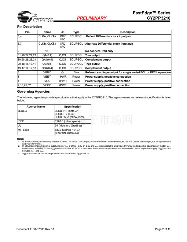
Hot-swappable/insertable
<50-ps output-to-output skew
<500-ps device-to-device skew
Less than 10-ps intrinsic jitter
500-ps propagation delay (typical)
Operation up to 1.5 GHz
PECL mode supply range: V
CC
= 2.375V to 3.465V with
V
EE
= 0V
ECL mode supply range: V
EE
= 鈥?.375V to 鈥?.465V with
V
CC
= 0V
Industrial temperature range: 鈥?0擄C to 85擄C
32-pin 1.4-mm TQFP package
Temperature compensation as 100K ECL
Description
The CY2PP3210 is a low-skew, low propagation delay dual
1-to-5 differential fanout buffer targeted to meet the require-
ments of high performance clock and data distribution applica-
tions. The device is implemented on SiGe technology and has
a fully differential internal architecture that is optimized to
achieve low signal skews at operating frequencies of up to 1.5
GHz.
The device features two differential input paths that are differ-
ential internally. The CY2PP3210 may function not only as a
differential clock buffer but also as a signal level translator and
fanout distributing a single-ended signal. An external bias pin,
VBB, is provided for an ECL/PECL single-ended or differential
signal to 10 ECL/PECL differential loads. In such an applica-
tion, the VBB pin should be connected to either one of the
CLKA# or CLKB# inputs and bypassed to V
CC
via a 0.01碌F
capacitor. Traditionally, in ECL, it is used to provide the refer-
ence level to a receiving single-ended input that might have a
different self bias point.
Since the CY2PP3210 introduces negligible jitter to the timing
budget, it is the ideal choice for distributing high-frequency,
high-precision clocks across back-planes and boards in
communication systems. Furthermore, advanced circuit
design schemes, such as internal temperature compensation,
ensure that the CY2PP3210 delivers consistent, guaranteed
performance over different platforms.
Block Diagram
QA0
QA0#
QA1
QA1#
CLKA
CLKA#
VCC
Pin Configuration
QA2
QA2#
QA3
QA3#
QA4
QA4#
QB0
QB0#
QB1
QB1#
QB2
QB2#
QB3
QB3#
QB4
QB4#
VBB
VCC
N.C.
CLKA
CLKA#
VBB
CLKB
CLKB#
VEE
1
2
3
4
5
6
7
8
32
31
30
29
28
27
26
25
VCCO
QA0
QA0#
QA1
QA1#
QA2
QA2#
VCCO
CY2PP3210
24
23
22
21
20
19
18
17
QA3
QA3#
QA4
QA4#
QB0
QB0#
QB1
QB1#
CLKB
CLKB#
VCC
Cypress Semiconductor Corporation
Document #: 38-07508 Rev. *A
鈥?/div>
3901 North First Street
鈥?/div>
San Jose
,
CA 95134
鈥?/div>
408-943-2600
Revised March 31, 2003
VCCO
QB4#
QB4
QB3#
QB3
QB2#
QB2
VCCO
9
10
11
12
13
14
15
16


 1
1
 2
2
 3
3
 4
4
 5
5
 6
6
 7
7
 8
8
 9
9
 10
10
 11
11
