COMLINK鈩?SERIES
CY2CC1910
1:10 Clock Fanout Buffer with Output Enable
Features
鈥?Low-voltage operation
鈥?Full-range support:
鈥?3.3V
鈥?2.5V
鈥?1.8V
鈥?1:10 fanout
鈥?Drives either a 50-Ohm or 75-Ohm load
鈥?Over voltage tolerant input hot swappable
鈥?Low-input capacitance
鈥?Low-output skew
鈥?Low-propagation delay
鈥?Typical (tpd < 4 ns)
鈥?High-speed operation:
鈥?100 MHz@1.8V
鈥?200 MHz@2.5V/3.3V
鈥?Industrial versions available
鈥?Available packages include: SOIC, SSOP
Description
The Cypress series of network circuits are produced using
advanced 0.35-micron CMOS technology, achieving the
industries fastest logic and buffers.
The Cypress CY2CC1910 fanout buffer features one input and
ten outputs. Ideal for conversion from/to 3.3V/2.5V/1.8V.
Designed for data communications clock management appli-
cations, the large fanout from a single input reduces loading
on the input clock.
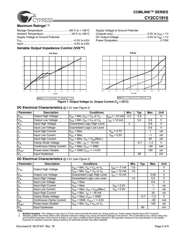
Cypress employs unique AVCMOS-type outputs VOI鈩?/div>
(Variable Output Impedance) that dynamically adjust for
variable impedance matching and eliminate the need for
series damping resistors; they also reduce noise overall.
Block Diagram
5
OE#
AVCMOS
23
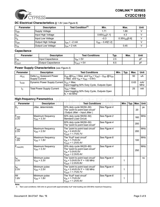
Pin Configuration
Q1
GND
Q10
VDD
Q9
OE#
IN
GND
GND
Q8
VDD
Q7
GND
21
Q2
19
VDD
18
Q3
Q4
16
3,10
15,22
6
IN
AVCMOS
Q5
1,12,13
17,24
14
Q6
11
1
2
3
4
5
6
7
8
9
10
11
12
24
23
22
21
20
19
18
17
16
15
14
13
CY2CC1910
GND
Q1
VDD
Q2
GND
Q3
Q4
GND
Q5
VDD
Q6
GND
24 pin SOIC/SSOP
Q7
9
GND
4
Q8
Q9
2
Q 10
OUTPUT
(AVCMOS)
Pin Description
Pin Number
1, 7, 8, 12, 13, 17, 20, 24
3,10,15,22
5
6
2, 4, 9, 11, 14, 16, 18, 19, 21, 23
Pin Description
G
ND
Ground
Power
V
DD
Power Supply
Power
OE#
Output Enable
LVTTL/LVCMOS
IN
Input
LVTTL/LVCMOS
Q10, Q9, Q8, Q7, Q6, Q5, Q4, Q3, Q2, Q1 Output
AVCMOS
鈥?/div>
3901 North First Street
鈥?/div>
San Jose
鈥?/div>
CA 95134 鈥?408-943-2600
Revised December 26, 2002
Pin Name
Cypress Semiconductor Corporation
Document #: 38-07347 Rev. *B


 1
1
 2
2
 3
3
 4
4
 5
5
 6
6
 7
7
 8
8
