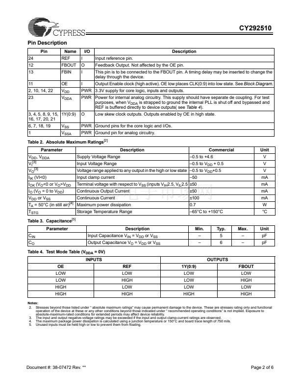
designed for registered SDRAM DIMM applications 鈥?/div>
JEDEC-JC42.5-compliant
鈥?Externally controllable output delay
鈥?Output enable/disable control
鈥?24-pin TSSOP package
Description
The CY292510 is a 3.3V zero delay buffer designed to
distribute high-speed clocks in PC, workstation, datacom,
telecom, and other high-performance applications. It is ideal
for use in SDRAM memory applications, and conforms to the
JEDEC JC40/JC42.5 specification supporting SDRAM DIMM
applications.
The CY292510 has one bank of outputs with output enable
control. Input-to-output skew can be adjusted by varying
load/delay on feedback path. When OE is low, clock outputs
are forced low. V
DDA
can be strapped low to force device into
test mode. See
Table 4.
Table 1. Function Table
[1]
OE
LOW
HIGH
1Y(0:9) Outputs
LOW
REF
FBOUT
REF
REF
Block Diagram
Pin Configuration
FBOUT
1Y0
1Y1
1Y2
1Y3
PLL
1
MUX
0
SEL
FBIN
REF
VDDA
1Y4
1Y5
1Y6
1Y7
1Y8
1Y9
OE
V
SSA
V
DD
1Y0
1Y1
1Y2
V
SS
V
SS
1Y3
1Y4
V
DD
OE
FBOUT
1
2
3
4
5
6
7
8
9
10
11
12
24
23
22
21
20
19
18
17
16
15
14
13
REF
V
DDA
V
DD
1Y9
1Y8
V
SS
V
SS
1Y7
1Y6
1Y5
V
DD
FBIN
Note:
1. See
Table 4
for additional logic configurations. REF is fixed frequency input.
Cypress Semiconductor Corporation
Document #: 38-07472 Rev. **
鈥?/div>
3901 North First Street
鈥?/div>
San Jose
鈥?/div>
CA 95134 鈥?408-943-2600
Revised October 11, 2002


 1
1
 2
2
 3
3
 4
4
 5
5
 6
6
