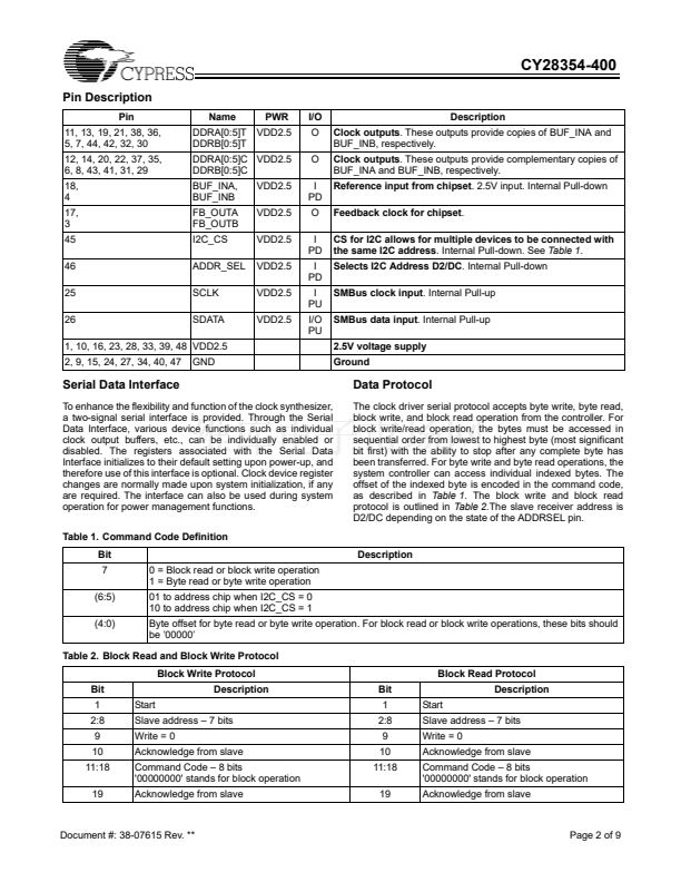
CY28354-400
273-MHz 24-Output Buffer for Four DDR
DIMMS for VIA Chipsets Support
Features
鈥?Supports VIA PRO 266, KT266 and P4x266
鈥?Dual 1- to 12-output buffer/driver
鈥?Supports up to 4 DDR DIMMs
鈥?Outputs are individually enabled/disabled
鈥?Low-skew outputs (< 75ps)
鈥?Supports 266-MHz, 333-MHz and 400-MHz DDR SDRAM
鈥?SMBus Read and Write support
鈥?Space-saving 48-pin SSOP package
Functional Description
The CY28354-400 is a 2.5V buffer designed to distribute
high-speed clocks in PC applications. The part has 24 outputs.
Designers can configure these outputs to support four unbuf-
fered DDR DIMMS or to support 3 unbuffered standard
SDRAM DIMMs and 2 DDR DIMMS. The CY28354-400 can
be used in conjunction with the W250 or similar clock synthe-
sizer for the VIA Pro 266, KT266 and P4X266 chipsets.
The CY28354-400 also includes an SMBus interface which
can enable or disable each output clock. On power-up, all
output clocks are enabled.
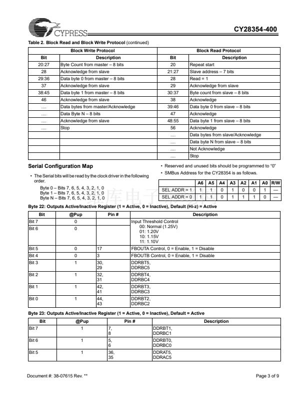
Block Diagram
BUF_INA
FB_OUTA
DDRAT0
DDRAC0
DDRAT1
DDRAC1
DDRAT2
DDRAC2
DDRAT3
DDRAC3
DDRAT4
DDRAC4
DDRAT5
DDRAC5
DDRBT0
DDRBC0
DDRBT1
DDRBC1
DDRBT2
DDRBC2
DDRBT3
DDRBC3
DDRBT4
DDRBC4
DDRBT5
DDRBC5
FB_OUTB
Pin Configuration
SSOP
Top View
VDD2.5
GND
FB_OUTB
BUFF_INB
DDRBT0
DDRBC0
DDRBT1
DDRBC1
GND
VDD2.5
DDRAT0
DDRAC0
DDRAT1
DDRAC1
GND
VDD2.5
FB_OUTA
BUF_INA
DDRAT2
DDRAC2
DDRAT3
DDRAC3
VDD2.5
GND
1
2
3
4
5
6
7
8
9
10
11
12
13
14
15
16
17
18
19
20
21
22
23
24
48
47
46
45
44
43
42
41
40
39
38
37
36
35
34
33
32
31
30
29
28
27
26
25
ADDR_SEL
SDATA
SMBus
Decoding
SCLOCK
I2C_CS
VDD2.5
GND
ADDR_SEL
I2C_CS
DDRBT2
DDRBC2
DDRBT3
DDRBC3
GND
VDD2.5
DDRAT4
DDRAC4
DDRAT5
DDRAC5
GND
VDD2.5
DDRBT4
DDRBC4
DDRBT5
DDRBC5
VDD2.5
GND
SDATA
SCLK
BUFF_INB
Cypress Semiconductor Corporation
Document #: 38-07615 Rev. **
鈥?/div>
3901 North First Street
鈥?/div>
San Jose
,
CA 95134
鈥?/div>
408-943-2600
Revised December 8, 2003


 1
1
 2
2
 3
3
 4
4
 5
5
 6
6
 7
7
 8
8
 9
9
