CY28353-2
Differential Clock Buffer/Driver
Features
鈥?Phase-locked loop (PLL) clock distribution for double
data rate synchronous DRAM applications
鈥?Distributes one differential clock input to six differential
outputs
鈥?External feedback pins (FBINT, FBINC) are used to
synchronize the outputs to the clock input
鈥?Conforms to the DDRI specification
鈥?Spread Aware for electromagnetic interference (EMI)
reduction
鈥?28-pin SSOP package
Description
This PLL clock buffer is designed for 2.5 V
DD
and 2.5 AV
DD
operation and differential data input and output levels.
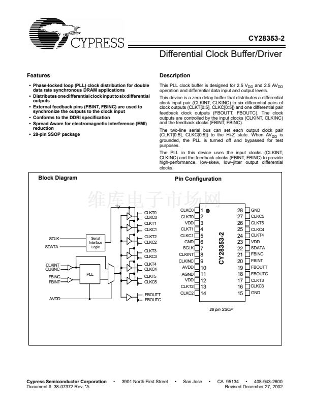
This device is a zero delay buffer that distributes a differential
clock input pair (CLKINT, CLKINC) to six differential pairs of
clock outputs (CLKT[0:5], CLKC[0:5]) and one differential pair
feedback clock outputs (FBOUTT, FBOUTC). The clock
outputs are controlled by the input clocks (CLKINT, CLKINC)
and the feedback clocks (FBINT, FBINC).
The two-line serial bus can set each output clock pair
(CLKT[0:5], CLKC[0:5]) to the Hi-Z state. When AV
DD
is
grounded, the PLL is turned off and bypassed for test
purposes.
The PLL in this device uses the input clocks (CLKINT,
CLKINC) and the feedback clocks (FBINT, FBINC) to provide
high-performance, low-skew, low鈥搄itter output differential
clocks.
Block Diagram
Pin Configuration
10
CLKT0
CLKC0
CLKT1
CLKC1
SCLK
SDATA
Serial
Interface
Logic
CLKC0
CLKT0
VDD
CLKT1
CLKC1
GND
SCLK
CLKINT
CLKINC
AVDD
AGND
VDD
CLKT2
CLKC2
CLKT2
CLKC2
CLKT3
CLKC3
CLKINT
CLKINC
FBINC
FBINT
PLL
CLKT4
CLKC4
CLKT5
CLKC5
FBOUTT
FBOUTC
1
2
3
4
5
6
7
8
9
10
11
12
13
14
28
27
26
25
24
23
22
21
20
19
18
17
16
15
GND
CLKC5
CLKT5
CLKC4
CLKT4
VDD
SDATA
FBINC
FBINT
FBOUTT
FBOUTC
CLKT3
CLKC3
GND
AVDD
28 pin SSOP
Cypress Semiconductor Corporation
Document #: 38-07372 Rev. *A
鈥?/div>
3901 North First Street
鈥?/div>
San Jose
鈥?/div>
CA 95134 鈥?408-943-2600
Revised December 27, 2002
CY28353-2


 1
1
 2
2
 3
3
 4
4
 5
5
 6
6
 7
7
 8
8
