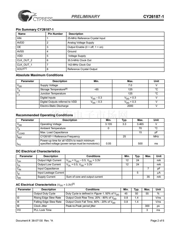
PRELIMINARY
CY26187-1
Broadcom Reference Design
Clock Generator
2CY26187-1-1CY2295
Features
鈥?Integrated phase-locked loop
鈥?Low skew, low jitter, high accuracy outputs
鈥?3.3V Operation
Broadcom Reference
Design
SDK5680
Benefits
Highest performance PLL tailored for multimedia applications
Meets critical timing requirements in complex system designs
Enables system and application compatibility
Part Number
CY26187-1
Outputs
2
Input Frequency
25 MHz
Output Frequencies
1 copy of 142 MHz, 1 copy 35.5 MHz (3.3V)
Logic Block Diagram - CY26187-1
XIN
XOUT
OSC.
Q
桅
VCO
P
OUTPUT
MULTIPLEXER
AND
DIVIDERS
CLK_OUT_1
CLK_OUT_2
PLL
OE
VDD
VSS
Pin Configuration
CY26187-1
8-pin SOIC
XIN
AVDD
OE
AVSS
1
2
3
4
8
7
6
5
XOUT
CLK_OUT_1
CLK_OUT_2
VDD
Cypress Semiconductor Corporation
Document #: 38-07130 Rev. *A
鈥?/div>
3901 North First Street
鈥?/div>
San Jose
鈥?/div>
CA 95134 鈥?408-943-2600
Revised December 14, 2002


 1
1
 2
2
 3
3
 4
4
 5
5
 6
6
