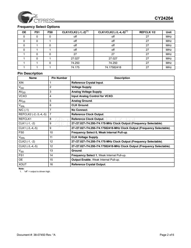
鈥?/div>
Integrated phase-locked loop (PLL)
Low jitter, high-accuracy outputs
VCXO with Analog Adjust
3.3V operation
Outputs
3
4
4
4
Input Frequency
27-MHz Crystal Input
27-MHz Crystal Input
27-MHz Crystal Input
27-MHz Crystal Input
Benefits
鈥?Internal PLL with up to 400MHz internal operation
鈥?Meets critical timing requirements in complex system
designs
鈥?Large 鹵150ppm range, better linearity
鈥?Enables application compatibility
Output Frequency Range
One copy of 27-MHz reference clock output, two copies of
27/27.027/74.250/74.175 MHz (frequency selectable)
Two copies of 27-MHz reference clock output, two copies of
27/27.027/74.250/74.175 MHz (frequency selectable)
Two copies of 27-MHz reference clock output, two copies of
27/27.027/74.250/74.17582418 MHz (frequency selectable)
Two copies of 27-MHz reference clock output, two copies of
27/27.027/74.250/74.17582418 MHz (frequency selectable,
Increased VCXO pull range)
Two copies of 27-MHz reference clock output, two copies of
27/27.027/74.250/74.17582418 MHz (frequency selectable,
Increased output drive strength)
Part Number
CY24204-1
CY24204-2
CY24204-3
CY24204-4
CY24204-5
4
27-MHz Crystal Input
Block Diagram
XIN
XOUT
VCXO
P
桅
VCO
OUTPUT
MULTIPLEXER
AND
DIVIDERS
CLK1
CLK2
REFCLK1
REFCLK2
(-2,-3,-4,-5)
Pin Configurations
16-pin TSSOP
XIN
VDD
AVDD
VCXO
AVSS
VSSL
NC
REFCLK1
1
2
16
15
XOUT
OE
FS1
VSS
CLK1
VDDL
FS0
CLK2
OSC.
Q
24204-1
3
4
5
6
7
8
14
13
12
11
10
9
PLL
FS0
FS1
OE
16-pin TSSOP
XIN
VDD
AVDD
VDDL
VDD
AVDD
AVSS
VSS
VSSL
1
16
XOUT
OE
FS1
VSS
CLK1
VDDL
FS0
CLK2
24204-2,3,4,5
2
3
4
5
6
7
8
15
14
13
12
11
10
9
VCXO
AVSS
VSSL
REFCLK2
REFCLK1
Cypress Semiconductor Corporation
Document #: 38-07450 Rev. *A
鈥?/div>
3901 North First Street
鈥?/div>
San Jose
,
CA 95134
鈥?/div>
408-943-2600
Revised September 8, 2003


 1
1
 2
2
 3
3
 4
4
 5
5
 6
6
