鈥?/div>
400-ps max Total Timing Budget錚?(TTB錚? window
10 LVPECL outputs
1 LVPECL differential input
Selectable output frequency range from 100 to 400 MHz
Multiply by 2 option
15-ps RMS Cycle-Cycle Jitter
Power-down mode
Lock indicator
3.3V power supply
Available in 48-pin QFN package
Overview
TheCY23020-3 is a high-performance 400-MHz LVPECL
Output phase-locked loop (PLL)-based zero delay buffer
(ZDB) designed for high- speed clock distribution applications.
The device features a guaranteed TTB window specifying all
occurrences of output clocks with respect to the input
reference clock across variations in voltage, temperature,
process, frequency, and ramp rate.
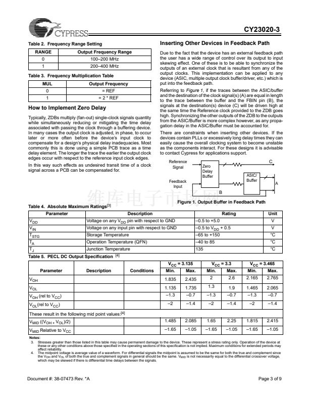
Additionally, the CY23020-3 can be used as a fan-out buffer
via the S[1:2] control pins. In this mode, the PLL is bypassed
and the reference clock is routed to the output buffers.
Block Diagram
48
Pin Configurations
47
V
D
D
46
F
B
I
N
+
45
F
B
I
N
-
44
N
C
43
L
O
C
K
42
V
D
D
C
41
G
N
D
C
40
R
E
F
-
39
R
E
F
+
38
V
D
D
37
Q
9
+
Q9- 36
GND 35
Q8- 34
Q8+ 33
VDD 32
LOCK
FBOUT+
FBOUT-
REF+
REF-
FBIN+
FBIN-
梅
1/
梅
2
1
2
3
4
5
6
FBOUT-
GND
Q1-
Q1+
VDD
Q2+
Q2-
GND
Q3-
Q3+
VDD
Q4+
梅
1
梅
2
PLL
Q1+
Q1-
Q2+
Q2-
Q3+
Q3-
Q4+
Q4-
F
B
O
U
T
+
CY23020-3
Q7+ 31
Q7- 30
GND 29
Q6- 28
Q6+ 27
VDD 26
Q5+ 25
S1:2
RANGE
MUL
Control
Logic
Q5+
Q4-
Q6+
Q6-
Q7+
Q7-
Q8+
Q8-
Q9+
Q9-
7
8
9
10
11
12
Q
4
-
G
N
D
S
2
S
1
M
U
L
R
A
N
G
E
18
G
N
D
C
19
V
D
D
C
20
V
D
D
C
21
G
N
D
C
G
N
D
Q
5
-
13
14
15
16
17
22
23
24
Cypress Semiconductor Corporation
Document #: 38-07473 Rev. *A
鈥?/div>
3901 North First Street
鈥?/div>
San Jose
,
CA 95134
鈥?/div>
408-943-2600
Revised June 5, 2003


 1
1
 2
2
 3
3
 4
4
 5
5
 6
6
 7
7
 8
8
 9
9
